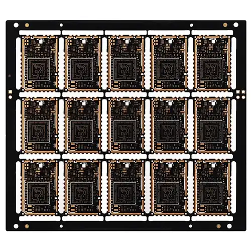
Name: Car driving recorder HDI PCB
Tier: 1+6+1
Sheet: EM825
Plate thickness: 1.6mm
Size: 242mm*165mm
Minimum blind hole: 0.1mm
Min Buried Via: 0.25mm
Minimum line width: 0.088mm
Minimum line spacing: 0.087mm
Surface Treatment: Immersion Gold
Outline tolerance: +/-0.1mm
Special requirements: L3-L6 resin plug holes
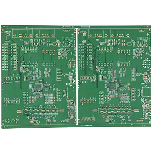
10-layer 1-stage HDI communication PCB
Name: 10-layer 1-stage HDI communication PCB
Layers: 1+8+1
Sheet: FR4 Tg170
Plate thickness: 1.2mm
Panel size: 110.8*94.8mm/4
Outer copper thickness: 35μm
Inner layer copper thickness: 18μm
Minimum through hole: 0.20mm
Minimum blind hole: 0.10mm
Minimum BGA: 0.20mm
Line width and line spacing: 2.5/2.2mil
Surface Treatment: Immersion Gold 2μ”+OSP
Application field: communication
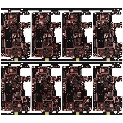
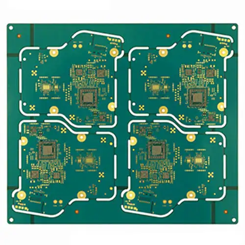
6L 2+N+2 HDI Communication PCB
Name: 6L 2+N+2 HDI Communication PCB
Model: 2+N+2 HDI communication PCB
Layers: 6Layers
Material: IT150
Construction : 2+2+2 HDI PCB
Finished Thickness: 0.8mm
Copper Thickness: 0.5OZ
Color: Green/White
Surface Treatment: Immersion Gold+OSP
Min Trace / Space: 3mil/3mil
Min Hole: Laser Hole 0.1mm
Application: Communication HDI PCB
Name: 6L 2+N+2 HDI WiFi Module PCB
Layers: 6Layers
Material: FR4 Tg170
Construction : 2+2+2 HDI PCB
Finished Thickness: 0.8mm
Copper Thickness: 1OZ
Color: Black/White
Surface Treatment: Immersion Gold+OSP
Min Trace / Space: 3mil/3mil
Min Hole: Laser Hole 0.1mm
Application: WiFi module PCB
Name: 6-layer 1-stage HDI PCB
Layers: 1+4+1
Sheet: FR4 Tg150
Plate thickness: 1.6mm
Panel size 105*95mm/1
Outer copper thickness: 35μm
Inner layer copper thickness: 30μm
Minimum through hole: 0.20mm
Minimum blind hole: 0.10mm
Minimum BGA: 0.20mm
Line width line spacing: 3/3mil
Surface Treatment: Immersion Gold 2μ”+OSP
Application field: industrial control
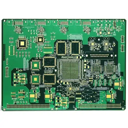
Name: 10-layer 3-stage HDI PCB
Layers: 3+4+3
Sheet: FR4 Tg170
Plate thickness: 1.2mm
Panel size: 126*118mm/4
Outer copper thickness: 35μm
Inner layer copper thickness: 18μm
Minimum through hole: 0.20mm
Minimum blind hole: 0.10mm
Minimum BGA: 0.25mm
Line width and spacing: 2.8/3.2mil
Surface Treatment: Immersion Gold 2μ”+OSP
- HDI PCB Capability
- PCB manufacturing equipment
Introducing our high-density interconnect printed circuit boards (HDI PCB), the epitome of cutting-edge technology in the world of electronics. Designed to meet the demands of modern electronic devices, our HDI PCBs offer superior performance, reliability, and miniaturization capabilities.
Our HDI PCBs are meticulously engineered using advanced manufacturing processes and materials, resulting in a compact design with highly efficient interconnections.
These PCBs boast a high circuit density, enabling the integration of numerous components within a smaller footprint. Whether you are working on smartphones, tablets, wearable devices, or any other compact electronic device, our HDI PCBs provide the ideal solution.
Advantages of HDI PCB:
- Enhanced Miniaturization: HDI PCBs are renowned for their ability to pack more circuitry into smaller form factors. By utilizing advanced microvia and fine-pitch technologies, HDI PCBs significantly reduce the overall size and weight of electronic devices, allowing for sleek and compact designs.
- Increased Signal Integrity: With HDI PCBs, signal integrity is greatly improved. The shorter trace lengths and reduced electromagnetic interference (EMI) result in minimal signal loss and noise, ensuring reliable and high-quality performance of the electronic device.
- Improved Electrical Performance: HDI PCBs offer excellent electrical performance due to their optimized routing and minimized parasitic capacitance and inductance. This leads to faster signal propagation and reduced power consumption, resulting in enhanced overall device efficiency.
- Enhanced Reliability: The advanced manufacturing techniques used in HDI PCBs ensure a high level of reliability and durability. These PCBs are resistant to thermal stress, vibration, and mechanical strain. It also makes them ideal for applications that require long-term reliability, such as automotive electronics and medical devices.
- Design Flexibility: HDI PCBs provide greater design flexibility, allowing for more complex and advanced circuitry designs. This flexibility enables the integration of multiple functionalities within a single board. It also reduces the need for additional PCBs and enhancing overall system performance.
| HDI (High Density Interconnect) PCB Process Capability | ||
| Item | batch | Template |
| layers | 4-16 Layers | 4-24 Layers |
| Plate thickness range | 0.6-3.2mm | 0.4-6.0mm |
| highest order | 4+N+4 | Any layer innterconnected |
| Minimum laser hole | 4mil (0.1mm) | 3mil (0.075mm) |
| Laser process | CO2 Laser Machine | CO2 Laser Machine |
| Tg value | 140/150/170°C | 140/150/170°C |
| hole copper | 12-18μm | 12-18μm |
| Impedance tolerance | +/-10% | +/-7% |
| interlayer alignment | +/-3mil | +/-2mil |
| Solder Mask Alignment | +/-2mil | +/-1mil |
| Minimum line width/line spacing | 2.5/2.5mil | 2.0/2.0mil |
| Smallest grommet | 2.5mil | 2.5mil |
| Minimum through hole | 8mil (0.2mm) | 6mil(0.15mm) |
| smallest micropore | 4.0mil | 3.0mil |
| Minimum media thickness | 3.0mil | 2.0mil |
| Minimum pad | 12mil | 10mil |
| Micropore Aperture Aspect Ratio | 1:1 | 1:2:1 |

PCB Drilling machine

PCB pattern plating line

PCB solder mask expose machine

PCB pattern expose machine

Strip film etching line

Solder mask screen silk print machine

Solder mask scrubbing line

PCB Flying Probe Test (FPT)

Fully automatic exposure machine

we provide 24-hour service and support, you will receive a reply to your question within 2 hours and a quotation within 24 hours.

Own PCB factory of 50,000 square meters, the monthly output can reach 60,000 square meters, no minimum PCB order requirements

Before the official production of the PCB, we will conduct a free DFM review service and support free Allegro, Altium, Protel, PADS, OBD, Gerber and other formats.

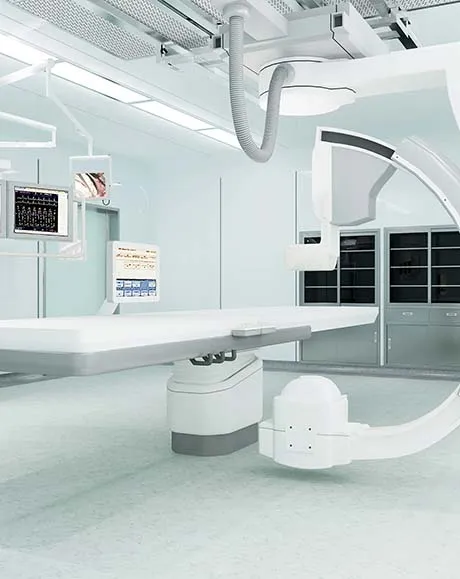
We can provide you with high frequency, high TG, high CTI, buried blind via, aluminum based PCB manufacturing, the quality is fully compliant with IPC 610-D standard, testing and quality assurance
Leadsintec provides Car driving recorder HDI PCB services. This is a PCBA one-stop assembly factory wi...
We support 10-layer 1-stage HDI communication PCB business, Leadsintec is a professional one-stop PCBA...
Leadsintec supports 6L 2+N+2 HDI Communication PCB business, we are a professional PCBA one-stop assem...
We provide 6L 2+N+2 HDI WiFi Module PCB services. Leadsintec is your one stop turnkey PCB assembly fac...
We support 6-layer 1-stage HDI PCB business, Leadsintec is a professional one-stop PCBA service factor...
Leadsintec provides 10-layer 3-stage HDI PCB services. This is a PCBA one-stop assembly factory with s...