

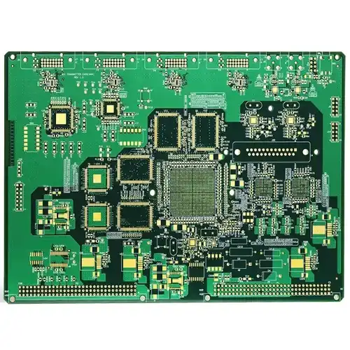
10-layer 1-stage HDI communication PCB
Name: 10-layer 1-stage HDI communication PCB
Layers: 1+8+1
Sheet: FR4 Tg170
Plate thickness: 1.2mm
Panel size: 110.8*94.8mm/4
Outer copper thickness: 35μm
Inner layer copper thickness: 18μm
Minimum through hole: 0.20mm
Minimum blind hole: 0.10mm
Minimum BGA: 0.20mm
Line width and line spacing: 2.5/2.2mil
Surface Treatment: Immersion Gold 2μ”+OSP
Application field: communication
The 10-Layer 1-Stage HDI Communication PCB is an advanced printed circuit board designed specifically for communication applications that require high-density interconnect (HDI) technology. It offers superior signal integrity, increased functionality, and enhanced reliability. This also makes it well-suited for use in telecommunications, networking, and other communication systems.
Technical features:
50 Ω Antenna, 90Ω & 100Ω Differential Impedance
Application of 10-layer 1-stage HDI communication PCB:
Cell Phones, Tablets, Ultrabooks, E-Readers, MP3 Players, GPS, Portable Game Consoles, DSCs, Cameras, LCD TVs, POS Terminals
HDI PCBs are widely used to reduce the weight and overall size of products, as well as improve the electrical performance of devices.
HDI PCBs also plays an important role in medical equipment as well as various electronic aircraft components. The possibilities for high-density interconnect 10-layer 1-stage communication PCB technology seem almost limitless.
Name: 10-layer 1-stage HDI communication PCB
Layers: 1+8+1
Sheet: FR4 Tg170
Plate thickness: 1.2mm
Panel size: 110.8*94.8mm/4
Outer copper thickness: 35μm
Inner layer copper thickness: 18μm
Minimum through hole: 0.20mm
Minimum blind hole: 0.10mm
Minimum BGA: 0.20mm
Line width and line spacing: 2.5/2.2mil
Surface Treatment: Immersion Gold 2μ”+OSP
Application field: communication
- Previous: 6L 2+N+2 HDI Communication PCB
- Next: Car driving recorder HDI PCB

