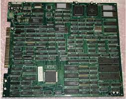
Medical Ultrasound System PCB Assembly -Leadsintec
Name: Medical Ultrasound System PCB Assembly -Leadsintec
Origin: China
Certified: UL, CE, RoHS
Surface Finishing: Immersion Gold
Solder mask color: Blue. green. red. black. white. etc
Base Material: FR-4
Copper Thickness: 1 oz, 1 Oz
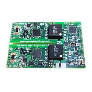
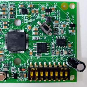
Wearble Medical PCB Assembly Device – For Fitness
Name: Wearble Medical PCB Assembly Device – For Fitness
Origin: China
Certified: UL, CE, RoSH
Number of Layers: 12-layer
Board Thickness: 0.2-3 MM, 1.6mm-3.2mm
Surface Finishing: HASL LF; ENIG; OSP; Hard Gold; Immersion Tin ;ENEPIG
Copper Thickness: 0-13 OZ Cu
Implantable Device PCB Assembly- Medical PCB
Name: Implantable Device PCB Assembly- Medical PCB
Origin: China
Certified: UL, CE, RoSH
Number of Layers: 12-layer
Copper Thickness: 0-13 OZ Cu
Surface Finishing: HASL LF; ENIG; OSP; Hard Gold; Immersion Tin ;ENEPIG
Board Thickness:0.2-3 MM, 1.6mm-3.2mm
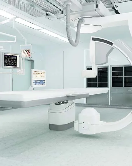
Scanning Device Medical PCB – One Stop Service in China
Name: Scanning Device Medical PCB – One Stop Service in China
Origin: China
Certified: UL, CE, RoSH
Copper Thickness: 1 oz
Surface Finishing: ENIG, HASL, OSP, etc.
Solder Mask: Blue
Layers: 4 Layers
Monitor PCB Assembly Medical Device -Leadsintec
Name: Monitor PCB Assembly Medical Device -Leadsintec
Origin: China
Certified: UL, CE, RoSH
Board Thickness: 0.2mm-7.0mm
Surface Finishing: HASL\OSP\immersion Gold
Copper Thickness: custom
Solder mask color: Blue. green. red.
Application: Electronics Device
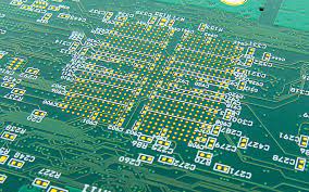
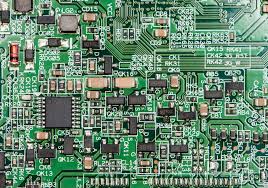
LAB analysis Medical PCB Assembly – PCBA manufacturer
Name: LAB analysis Medical PCB Assembly – PCBA manufacturer
Origin: China
Certified: UL, CE, RoSH
Copper Thickness: 4 oz
Surface Finishing: HASL ,OSP ,ENIG, Immersion Gold …
Layer Counts: 1–20L
Board Thickness: 0.4mm–3.2mm
- PCB Assembly Capability
- PCB Assembly Equipment
Medical PCB Assembly is a specialized electronic manufacturing service that focuses on the assembly of printed circuit boards (PCBs) for medical applications. It involves the precise and reliable assembly of PCBs that meet the stringent requirements of the medical industry, including accuracy, reliability, safety, and compliance with medical regulations and standards.
Medical PCB plays a crucial role in the production of electronic devices and equipment used in various medical applications, such as diagnostic equipment, patient monitoring systems, imaging devices, therapeutic devices, and more. These assemblies are designed to withstand rigorous operating conditions, ensure patient safety, and provide reliable performance in critical medical environments.
Key Features and Advantages of Medical PCB Assembly:
- Compliance with Medical Standards: Medical Assembly adheres to specific medical standards and regulations, such as ISO 13485 and IEC 60601, to ensure that the assembled PCBs meet the required safety and quality standards for medical devices. This includes proper documentation, traceability, risk management, and quality control processes.
- Precision and Accuracy: Medical PCB focuses on achieving high precision and accuracy in the assembly process. This includes precise placement of components, accurate soldering, and meticulous quality control measures to ensure the reliable performance of the medical devices and equipment.
- Component Selection and Traceability: Medical PCB carefully selects components that are suitable for medical applications, considering factors such as reliability, longevity, and biocompatibility. It also ensures component traceability, maintaining records of component sources, lot numbers, and certifications for quality control and future reference.
- EMI/EMC Compliance: Medical devices often operate in sensitive medical environments and require compliance with electromagnetic interference (EMI) and electromagnetic compatibility (EMC) standards. Medical PCB Assembly incorporates shielding techniques, grounding strategies, and appropriate component placement to minimize EMI and ensure reliable operation without interfering with other medical equipment.
- Sterilization Compatibility: Some medical devices and equipment require sterilization processes. Medical PCB considers the compatibility of materials, components, and PCB finishes with various sterilization methods, such as steam sterilization, ethylene oxide (EO) sterilization, or gamma radiation sterilization.
| SMT capacity: 19 million points/day | ||
| Testing Equipment | X-RAY Nondestructive Tester, First Piece Tester, AOI Automatic Optical Tester, ICT Tester, BGA Rework Station | |
| Placement speed | Chip placement speed (at best conditions) 0.036 S/piece | |
| Mounted Component Specifications | Pasteable smallest package | |
| Minimum device accuracy | ||
| IC type chip accuracy | ||
| Mounted PCB Specifications | Substrate size | |
| Substrate thickness | ||
| throw rate | 1. Resistance-capacitance ratio 0.3% | |
| 2. IC type without throwing material | ||
| Board Type | POP/common board/FPC/rigid-flex board/metal substrate | |
| DIP daily production capacity | ||
| DIP plug-in production line | 50000 points/day | |
| DIP post welding production line | 20000 points/day | |
| DIP test production line | 50000pcs PCBA/day | |
| Assembly processing capability | ||
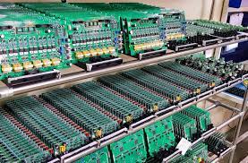
| The company has more than 10 advanced assembly production lines, dust-free and anti-static air-conditioning workshop, TP dust-free workshop, equipped with aging room, test room, functional test isolation room, advanced and perfect equipment, can carry out various product assembly, packaging, testing, Aging, etc. production. Monthly production capacity can reach 150,000 to 300,000 sets/month | ||
| PCBA processing capability | ||
| project | Mass processing capability | Small batch processing capability |
| Number of layers (max) | 2-18 | 20-30 |
| Plate type | FR-4, Ceramic Sheet, Aluminum Base Sheet PTFE, Halogen Free Sheet, High Tg Sheet | PTFE, PPO, PPE |
| Rogers,etc Teflon | E-65, ect | |
| Sheet mixing | 4 layers – 6 layers | 6th floor – 8th floor |
| biggest size | 610mm X 1100mm | / |
| Dimensional Accuracy | ±0.13mm | ±0.10mm |
| Plate thickness range | 0.2mm–6.00mm | 0.2mm–8.00mm |
| Thickness tolerance ( t≥0.8mm) | ±8% | ±5% |
| Thickness tolerance (t<0.8mm) | ±10% | ±8% |
| Media thickness | 0.076mm–6.00mm | 0.076mm–0.100mm |
| Minimum line width | 0.10mm | 0.075mm |
| Minimum spacing | 0.10mm | 0.075mm |
| Outer copper thickness | 8.75um–175um | 8.75um–280um |
| Inner layer copper thickness | 17.5um–175um | 0.15mm–0.25mm |
| Drilling hole diameter (mechanical drill) | 0.25mm–6.00mm | 0.15mm–0.25mm |
| Hole diameter (mechanical drill) | 0.20mm–6.00mm | 0.10mm–0.20mm |
| Hole Tolerance (Mechanical Drill) | 0.05mm | / |
| Hole tolerance (mechanical drill) | 0.075mm | 0.050mm |
| Laser Drilling Aperture | 0.10mm | 0.075mm |
| Plate thickness aperture ratio | 10:1 | 12:1 |
| Solder mask type | Photosensitive green, yellow, black, purple, blue, ink | / |
| Minimum Solder Mask Bridge Width | 0.10mm | 0.075mm |
| Minimum Solder Mask Isolation Ring | 0.05mm | 0.025mm |
| Plug hole diameter | 0.25mm–0.60mm | 0.60mm-0.80mm |
| Impedance tolerance | ±10% | ±5% |
| Surface treatment type | Hot air leveling, chemical nickel gold, immersion silver, electroplated nickel gold, chemical immersion tin, gold finger card board | Immersion Tin, OSP |

Automatic Solder Paste Printing Machine

AOI Optical Inspection

Smt High-Speed Placement Machine

Nitrogen Reflow Soldering

X-Ray

Three Anti-Paint Spraying Machine

SPI Solder Paste Thickness Tester

Automatic Wave Soldering Machine

First Article Inspection