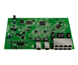
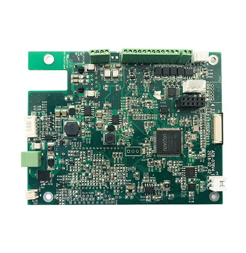
- PCB manufacturing capability
- PCB manufacturing equipment
Introducing our high-Tg (glass transition temperature) PCBs, designed to withstand elevated temperatures and provide exceptional thermal stability in demanding applications. Our high-Tg PCBs are built using specialized materials that offer enhanced mechanical and thermal properties. This also ensures reliable performance in high-temperature environments.
Our high-Tg PCBs are ideal for applications that require resistance to high-temperature soldering processes, elevated operating temperatures, or exposure to thermal stress. Whether you’re working on automotive electronics, industrial equipment, aerospace systems, or any other high-temperature application, our high-Tg PCBs are a reliable choice.
Our high-Tg PCBs provide design flexibility, enabling the integration of complex circuit layouts and multi-layer structures. They support fine-pitch components, high-density interconnections, and controlled impedance designs.
Advantages of High-Tg PCB:
- Elevated Temperature Resistance: High-Tg PCBs are specifically engineered to withstand elevated temperatures beyond the capabilities of standard PCB materials. They exhibit a higher glass transition temperature, typically above 170°C. It also ensures dimensional stability and mechanical integrity even under extreme thermal conditions.
- Enhanced Thermal Performance: High-Tg PCBs offer superior thermal conductivity and dissipation properties. They efficiently transfer heat away from heat-generating components. This also prevent it from overheating and ensuring the reliable operation of sensitive electronic devices in high-temperature environments.
- Resistance to Thermal Stress: High-Tg PCBs are less susceptible to thermal stress and mechanical failures caused by temperature variations. Their robust construction and specialized materials minimize the risk of delamination, warping, and solder joint failures, even during repeated thermal cycling or exposure to rapid temperature changes.
- Compatibility with High-Temperature Soldering Processes: High-Tg PCBs are designed to withstand the high temperatures associated with lead-free and high-temperature soldering processes. These PCBs exhibit excellent solderability and resistance to solder joint cracking or thermal fatigue.
- Reliability in Harsh Environments: High-Tg PCBs offer increased reliability in harsh operating environments. They can endure extreme temperature variations, high humidity, and exposure to chemicals or corrosive substances.
| Standard PCB Production Capability | |
| Feature | Capability |
| Quality Grade | Standard IPC 2 |
| Number of Layers | 1 – 32layers |
| Order Quantity | 1pcs – 10,000,000 pcs |
| Build Time | 2days – 5weeks (Expedited Service) |
| Material | FR-4 Standard Tg 150°C, FR4-High Tg 170°C, FR4-High-Tg 180°C, FR4-Halogen-free, FR4-Halogen-free & High-Tg |
| Board Size | Min 6*6mm | Max 600*700mm |
| Board size tolerance | ±0.1mm – ±0.3mm |
| Board Thickness | 0.4mm – 3.2mm |
| Board Thickness Tolerance | ±0.1mm – ±10% |
| Copper Weight | 0.5oz – 6.0oz |
| Inner Layer Copper Weight | 0.5oz – 2.0oz |
| Copper Thickness Tolerance | +0μm +20μm |
| Min Tracing/Spacing | 3mil/3mil |
| Solder Mask Sides | As per the file |
| Solder Mask Color | Green, White, Blue, Black, Red, Yellow |
| Silkscreen Sides | As per the file |
| Silkscreen Color | White, Blue, Black, Red, Yellow |
| Surface Finish | HASL – Hot Air Solder Leveling |
| Lead Free HASL – RoHS | |
| ENIG – Electroless Nickle/Immersion Gold – RoHS | |
| ENEPIG – Electroless Nickel Electroless Palladium Immersion Gold – RoHS | |
| Immersion Silver – RoHS | |
| Immersion Tin – RoHS | |
| OSP -Organic Solderability Preservatives – RoHS | |
| Min Annular Ring | 3mil |
| Min Drilling Hole Diameter | 6mil, 4mil-laser drill |
| Min Width of Cutout (NPTH) | 0.8mm |
| NPTH Hole Size Tolerance | ±.002″ (±0.05mm) |
| Min Width of Slot Hole (PTH) | 0.6mm |
| PTH Hole Size Tolerance | ±.003″ (±0.08mm) – ±4mil |
| Surface/Hole Plating Thickness | 20μm – 30μm |
| SM Tolerance (LPI) | .003″ (0.075mm) |
| Aspect Ratio | 1.10 (hole size: board thickness) |
| Test | 10V – 250V, flying probe or testing fixture |
| Impedance tolerance | ±5% – ±10% |
| SMD Pitch | 0.2mm(8mil) |
| BGA Pitch | 0.2mm(8mil) |
| Chamfer of Gold Fingers | 20, 30, 45, 60 |
| Other Techniques | Gold fingers |
| Blind and Buried Holes | |
| peelable solder mask | |
| Edge plating | |
| Carbon Mask | |
| Kapton tape | |
| Countersink/counterbore hole | |
| Half-cut/Castellated hole | |
| Press fit hole | |
| Via tented/covered with resin | |
| Via plugged/filled with resin | |
| Via in pad | |
| Electrical Test | |
PCB Drilling machine
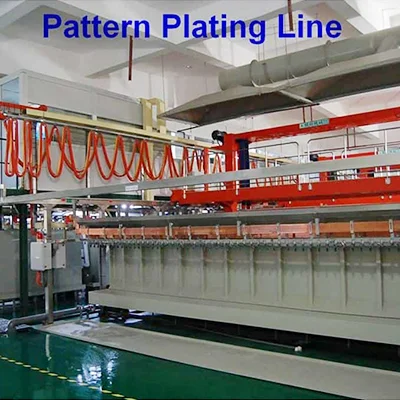
PCB pattern plating line
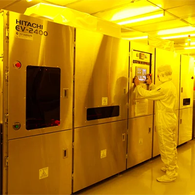
PCB solder mask expose machine
PCB pattern expose machine
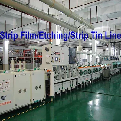
Strip film etching line
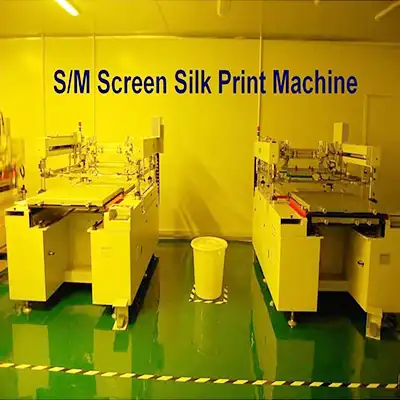
Solder mask screen silk print machine
Solder mask scrubbing line
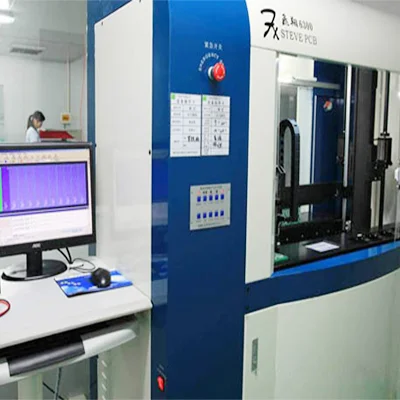
PCB Flying Probe Test (FPT)
Fully automatic exposure machine

