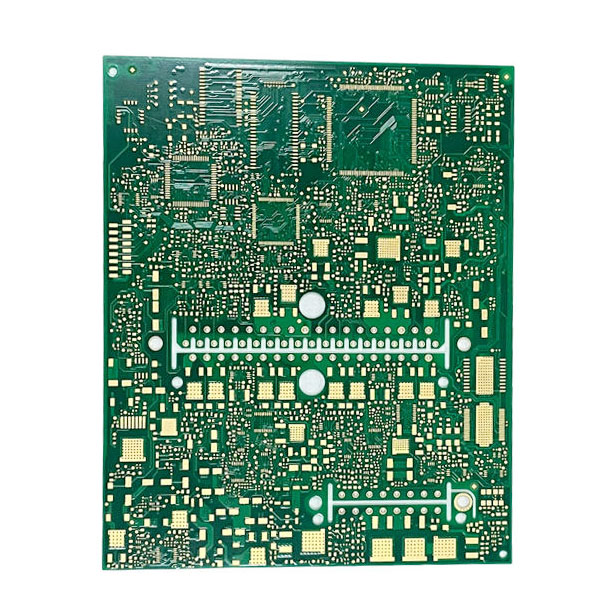
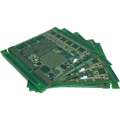
Multilayer PCB 8 layer ENIG PCB board for Automotive Customized
Name: Multilayer PCB
Applied for:: Portable DVD player, spa controller, LED lamp, hub
Layer: 8Layer Multilayer PCB
Solder Mask Color: Green/White/Blue/Red
Silk Screen Color: White/Black
Min Trace: 3mil(0.75mm)
Min Space: 3mil(0.75mm)
Application: Consumer electronics
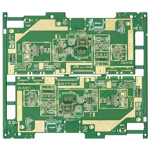
Multilayer Printed Circuit Board(PCB) Fabrication
Name: Multilayer PCB
Material: KB6061, S1141, S1000, IT180
Layer: 4Layer – 48Layer Multilayer PCB
Solder Mask Color: Green/White/Blue/Red
Silk Screen Color: White/Black
Finished Thickness: 0.3mm – 6.0mm
Copper Thickness: 0.5-6OZ
Surface Treatment: Immersion Gold/OSP/HASL
Min Trace: 3mil(0.75mm)
Min Space: 3mil(0.75mm)
Application: Consumer electronics
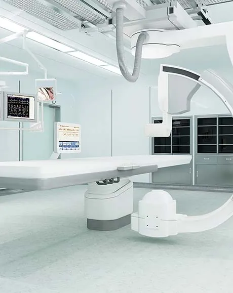
Name: Medical device PCB
Substrate: FR4
Laminate: 8L
Dielectric constant: 4.2
Plate thickness: 1.6MM
Outer copper foil thickness: 1oz
Inner copper foil thickness: 1oz
Minimum aperture: 0.2mm
Minimum line width: 0.1MM
Minimum line spacing: 0.1MM
Gold Thickness: 1U”
Application field: medical PCB
Name: 14-layer PCB circuit board
Layers: 14L
Sheet: FR4 Tg180
Plate thickness: 2.4mm
Panel size: 120*95mm/1
Outer copper thickness: 35μm
Inner layer copper thickness: 35μm
Minimum through hole: 0.20mm
Minimum BGA: 0.25mm
Line width line spacing: 3/3.2mil
Surface treatment: Immersion gold 2U”
Application field: automotive core PCB board
- Multilayer PCB Capability
- PCB manufacturing equipment
Introducing our multilayer PCB, designed to meet the increasing complexity and density requirements of modern electronic systems. Our multilayer PCBs offer enhanced functionality, improved signal integrity, and efficient use of space by incorporating multiple layers of conductive traces and insulating materials.
Our multilayer PCBs are suitable for a wide range of applications, including telecommunications, data storage, medical devices, aerospace, also consumer electronics, and more.
With their ability to accommodate high-speed signals, reduce electromagnetic interference, and provide design flexibility, our multilayer PCBs are the ideal choice for demanding electronic designs.
Key Features of Multilayer PCB:
- High Density and Space Optimization: Multilayer PCBs provide a higher level of component density and space optimization compared to single or double-sided PCBs. By stacking multiple layers of conductive traces and insulating materials, these PCBs allow for more compact designs, increased routing flexibility.
- Enhanced Signal Integrity: Multilayer PCBs offer improved signal integrity by providing dedicated signal layers and power/ground planes. The use of separate signal layers helps reduce crosstalk, noise, and electromagnetic interference (EMI), ensuring reliable signal transmission and also minimizing signal degradation in high-speed and high-frequency applications.
- Power Distribution and Grounding: Multilayer PCBs enable efficient power distribution and grounding. The inclusion of power and ground planes throughout the PCB ensures stable power supply and minimizes voltage drops. These planes also act as shielding layers, reducing electromagnetic emissions and enhancing system performance.
- Design Flexibility: Multilayer PCBs provide greater design flexibility compared to single or double-sided PCBs. They support complex circuitry, high-density component placement, and intricate routing patterns. This flexibility allows for the integration of advanced functionalities, such as high-speed interfaces, impedance matching, differential signaling, and RF/microwave circuitry.
- Reduced Electromagnetic Emissions: The use of dedicated ground and power planes in multilayer PCBs helps minimize electromagnetic emissions. This is crucial in applications where electromagnetic compatibility (EMC) is a concern, as it helps ensure compliance with regulatory standards and reduces the risk of interference with other electronic devices.
| Multilayer PCB Production Capability | |
| Item | Capability |
| Layer Count | 1-40layers |
| Base Material | KB、Shengyi、ShengyiSF305、FR408、FR408HR、IS410、FR406、GETEK、370HR、IT180A、Rogers4350B、Rogers4000、PTFE Laminates(Rogers series、Taconic series、Arlon series、Nelco series)、Rogers/Taconic/Arlon/Nelco laminate with FR-4 material(including partial Ro4350B hybrid laminating with FR-4) |
| Board Type | Backplane、HDI、High multi-layer 、blind&buried PCB、Embedded Capacitance、Embedded resistance board 、Heavy copper power PCB、Backdrill. |
| Board Thickness | 0.2-5.0mm |
| Copper Thickness | Min. 1/2 OZ, Max. 10 OZ |
| PTH Wall | 25um(1mil) |
| Maximum Board Size | 1100*500mm(43”*19”) |
| Min laser drilling size | 4mil |
| Min. Spacing/Tracing | 2.7mil/2.7mil |
| Solder Mask | Green, Black, Blue, Red, White, Yellow, Purple matte/glossy |
| Surface Treatment | Flash gold(electroplated gold)、ENIG、Hard gold、Flash gold、HASL Lead-free 、OSP、ENEPIG、Soft gold、Immersion silver、Immersion Tin、ENIG+OSP, ENIG+Gold finger, Flash gold(electroplated gold)+Gold finger, Immersion silver+Gold finger, Immersion Tin+Gold finger. |
| Min. Annular Ring | 3mil |
| Aspect ratio | 10:1(HASL Lead-free 、HASL Lead、ENIG、Immersion Tin、Immersion silver、ENEPIG);8:1(OSP) |
| Impedance control | ±5ohm(<50ohm), ±10%(≥50ohm) |
| Other Techniques | Blind/Buried Via |
| Gold Fingers | |
| Press Fit | |
| Via in Pad | |
| Electrical Test | |

PCB Drilling machine

PCB pattern plating line

PCB solder mask expose machine

PCB pattern expose machine

Strip film etching line

Solder mask screen silk print machine

Solder mask scrubbing line

PCB Flying Probe Test (FPT)

Fully automatic exposure machine

we provide 24-hour service and support, you will receive a reply to your question within 2 hours and a quotation within 24 hours.

Own PCB factory of 50,000 square meters, the monthly output can reach 60,000 square meters, no minimum PCB order requirements

Before the official production of the PCB, we will conduct a free DFM review service and support free Allegro, Altium, Protel, PADS, OBD, Gerber and other formats.

We can provide you with high frequency, high TG, high CTI, buried blind via, aluminum based PCB manufacturing, the quality is fully compliant with IPC 610-D standard, testing and quality assurance
Leadsintec provides Medical Equipment PCB services. This is a PCBA one-stop assembly factory with seni...
We are a professional PCBA one-stop assembly factory, Leadsintec supports 10-layer PCB circuit board b...
We are a professional PCBA one-stop assembly factory, Leadsintec supports 10-layer PCB circuit board b...