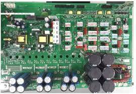
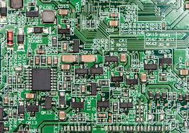
PCB & PCBA Solar Hybrid Inverter PCB Board
Name: PCB & PCBA Solar Hybrid Inverter PCB Board
Origin: China
Certified: UL, CE, RoHS
Solder mask color: Blue. green. red. black. white. etc
Layer: 1-24layers
Surface Finishing: HASL\OSP\immersion Gold
Copper Thickness: 1 oz
Base Material: FR-4/aluminum/ceramic/cem-3/FR-1
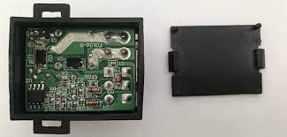
Sensor PCB Automotive Electronic PCBA
Name: Sensor PCB Automotive Electronic PCBA
Origin: China
Certified: UL, CE, RoHS
Surface Finishing: Lead-free HASL
Copper Thickness: 2 OZ
Board Thickness: customized
Solder mask: White Black Green Blue Red
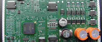
Automtive Control System Electronic PCBA for Suspension and Engine Functions
Name: Automtive Control System Electronic PCBA for Suspension and Engine Functions
Copper Thickness: 1 oz, 0.5 oz ~ 7.0 oz
Application: for Automtive Control System
Board Thickness: customized
Base Material: FR-4
Surface Finishing: HASL Lead Free
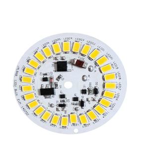
LED PCB Board for Automotive Electronics
Name: LED PCB Board for Automotive Electronics
Base Material: fr4/Aluminum
Copper Thickness: 1oz
Board Thickness: customized
Origin: China
Certified: UL, CE, RoHS
Application: Electronics Device
Solder mask color: Blue. green. red. black. white.etc
Display PCB for Cars – Leadsintec PCB Manufacturer
Name: Display PCB for Cars – Leadsintec PCB Manufacturer
Origin: China
Certified: UL, CE, RoHS
Base Material: FR-4
Copper Thickness: customized
Board Thickness: customized
Surface Finishing: HASL Lead Free
applications: for cars
- Description
PCB assembly, or Printed Circuit Board assembly, is the process of mounting and soldering electronic components onto a printed circuit board to create a functional electronic device or circuit. The PCB serves as the foundation for the electrical connections between components, providing a platform for the assembly of various electronic devices, ranging from simple toys to complex computer systems.
The PCB assembly process typically involves several steps:
- Component Placement: Electronic components, such as resistors, capacitors, integrated circuits, and connectors, are placed onto the PCB according to the circuit design. This step can be done manually or with the assistance of automated pick-and-place machines, depending on the complexity and volume of the assembly.
- Soldering: Once the components are placed on the PCB, they are soldered onto the board to establish electrical connections. Soldering can be done through wave soldering, reflow soldering, or hand soldering, depending on the specific requirements of the assembly.
- Inspection: After soldering, the assembled PCB undergoes inspection to ensure that all components are properly soldered and positioned according to the design specifications. Various techniques, such as visual inspection, automated optical inspection (AOI), and X-ray inspection, may be used to detect any defects or inconsistencies.
- Testing: Once the inspection is complete, the assembled PCB is tested to verify its functionality and performance. This may involve functional testing, electrical testing, and other tests to ensure that the circuit operates as intended and meets quality standards.
- Final Assembly: After testing, the PCB may undergo additional assembly steps, such as the installation of connectors, switches, and other external components required to complete the electronic device.
Additional types of PCB assembly include:
- Ball Grid Array (BGA) Assembly: BGA is a type of surface mount packaging used for integrated circuits. Instead of pins, BGA packages use solder balls arranged in a grid pattern on the underside of the component.
- Chip-on-Board (COB) Assembly: In COB assembly, bare semiconductor chips are directly mounted onto the PCB substrate and then wire bonded or encapsulated. This method is commonly used in applications where space-saving and cost-efficiency are priorities.
- Flexible PCB Assembly: Flexible PCBs, also known as flex circuits, are made of flexible plastic substrates. Components can be mounted on these substrates using various assembly techniques, including surface mount and through-hole methods.
- Rigid-Flex PCB Assembly): Rigid-flex PCBs combine rigid and flexible substrates into a single board. This allows for more compact and lightweight designs, especially in applications where space is limited or mechanical flexibility is required.
- Wire Harness Assembly: Wire harness assembly involves the integration of wires, cables, and connectors onto the PCB to facilitate interconnection between various electronic components or subsystems. This method is common in complex electronic systems such as automobiles and industrial machinery.
Your outline of the PCB assembly process is quite comprehensive. Here’s a bit more detail on each step:
- Component Procurement: This involves sourcing electronic components from suppliers. It’s crucial to ensure that components are genuine, meet required specifications, and are available in the quantities needed for production.
- Stencil Printing: Solder paste, a mixture of flux and tiny solder particles, is applied onto the PCB through a stencil. The stencil defines where solder paste will be deposited onto the board’s surface, corresponding to the locations where components will be placed.
- Component Placement: Once the solder paste is applied, components are placed onto the PCB. This can be done manually for prototypes or small-volume production, but automated pick-and-place machines are typically used for larger-scale manufacturing. These machines can quickly and accurately position components onto the PCB based on digital design files.
- Soldering: After components are placed, the PCB goes through a soldering process to permanently bond them to the board. There are two main methods for soldering: reflow soldering and wave soldering. Reflow soldering involves heating the entire PCB to melt the solder paste, creating electrical connections. Wave soldering is used primarily for through-hole components, where the PCB is passed over a wave of molten solder.
- Inspection: Once soldering is complete, the assembled PCB undergoes inspection to ensure quality and reliability. This can include visual inspection, automated optical inspection (AOI), or X-ray inspection to detect defects such as solder bridges, insufficient solder joints, or misaligned components.
- Testing and Quality Assurance: After inspection, the assembled PCBs are subjected to functional and electrical tests to verify that they meet performance specifications. This may involve powering up the PCB and running diagnostic tests to ensure proper functionality.
- Packaging and Shipping: Once PCBs pass all quality checks, they are packaged securely to protect them during transportation and storage. Packaging may vary depending on factors such as size, fragility, and shipping requirements. Finally, the assembled PCBs are shipped to customers or other facilities for further integration into larger electronic systems.
These are indeed key benefits of PCB assembly. Here’s a bit more detail on each:
- Increased Efficiency: PCB assembly streamlines the production process by automating repetitive tasks, resulting in higher throughput and lower labor costs. Mass production of electronic circuits becomes feasible, leading to economies of scale and reduced manufacturing lead times.
- High Precision: Automated assembly machines ensure precise component placement with tight tolerances, minimizing the risk of errors that could compromise the functionality or reliability of the final product. This precision is especially crucial for complex circuit designs with densely packed components.
- Better Reliability: Machine assembly processes, coupled with stringent quality control measures, contribute to improved reliability and durability of PCB assemblies. Consistent soldering and inspection techniques help identify and rectify defects early in the manufacturing process, resulting in fewer field failures and warranty claims.
- Space Saving: Surface mount technology (SMT) allows for the mounting of components directly onto the surface of the PCB, eliminating the need for bulky through-holes. This miniaturization enables the design of smaller and more compact electronic devices without compromising functionality, making them ideal for applications where space is limited.
- Flexibility: PCB assembly supports a wide range of component types, sizes, and technologies, offering designers the flexibility to create custom solutions tailored to specific requirements.