

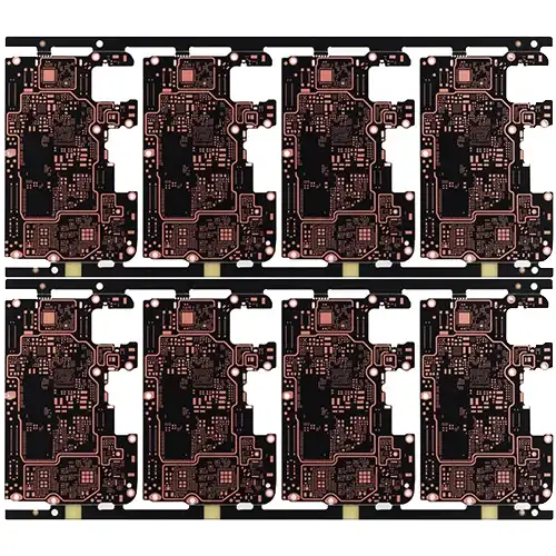
6L 2+N+2 HDI Communication PCB
Name: 6L 2+N+2 HDI Communication PCB
Model: 2+N+2 HDI communication PCB
Layers: 6Layers
Material: IT150
Construction : 2+2+2 HDI PCB
Finished Thickness: 0.8mm
Copper Thickness: 0.5OZ
Color: Green/White
Surface Treatment: Immersion Gold+OSP
Min Trace / Space: 3mil/3mil
Min Hole: Laser Hole 0.1mm
Application: Communication HDI PCB
The 6L 2+N+2 HDI Communication PCB (Printed Circuit Board) is a high-density interconnect (HDI) board specifically designed for communication applications. It offers advanced functionality and reliability, making it suitable for use in various communication systems such as routers, switches, telecommunication equipment, and networking devices.
Advantages
Advantages of the 6L 2+N+2 HDI Communication PCB include:
- High Signal Density: The HDI technology used in this PCB allows for a higher signal density, enabling more components to be integrated into a smaller space. This results in a more compact and efficient communication system design.
- Improved Signal Integrity: The 2+N+2 structure and advanced HDI routing techniques minimize signal distortion, noise, and electromagnetic interference. This ensures improved signal integrity and reduces the chances of data corruption or loss during communication.
- Enhanced Electrical Performance: The use of high-quality materials and the optimized layer configuration of the PCB contribute to enhanced electrical performance. It provides better impedance control, lower signal loss, and also improved transmission speeds, allowing for reliable and high-speed data transfer.
- Design Flexibility: The 6L 2+N+2 HDI Communication PCB offers design flexibility, allowing for customization according to specific requirements. This flexibility also enables engineers to design and optimize the PCB layout, component placement, and routing for optimal performance and functionality.
- Reliability and Durability: The PCB is manufactured using high-quality materials and undergoes rigorous testing to ensure reliability and durability. It can withstand demanding environmental conditions, temperature variations, and mechanical stress, providing long-term performance and stability.
Features of 6L 2+N+2 HDI Communication PCB:
- For BGAs with smaller ball pitch and higher I/O count
- Increase routing density in complex designs
- Sheet Capability
- Lower Dk/Df material for better signal transmission performance
- copper filled vias
- Applications: Mobile phones, PDAs, UMPCs, portable game consoles, digital cameras, camcorders
Name: 6L 2+N+2 HDI Communication PCB
Model: 2+N+2 HDI communication PCB
Layers: 6Layers
Material: IT150
Construction : 2+2+2 HDI PCB
Finished Thickness: 0.8mm
Copper Thickness: 0.5OZ
Color: Green/White
Surface Treatment: Immersion Gold+OSP
Min Trace / Space: 3mil/3mil
Min Hole: Laser Hole 0.1mm
Application: Communication HDI PCB
- Previous: 6L 2+N+2 HDI WiFi Module PCB
- Next: 10-layer 1-stage HDI communication PCB

