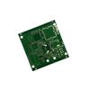
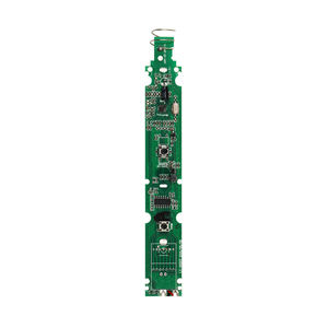
Prototype PCB Assembly for Home Appliances
Name: Prototype PCB Assembly for Home Appliances
Origin: China
Certified: UL, CE, RoHS
Surface Finishing: HASL ,OSP ,ENIG, Immsersion Gold
Layer Counts: 1–20L
Base Material: FR4,High-TG FR4,CEM3,aluminum,High Frequency(Rogers,Taconic,Aron,PTFE,F4B)
Solder mask:Green, Blue, Black, White, Yellow, Red, Matt Green, Matt Black, Matt Blue
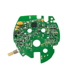
Consumer Prototype PCB Assembly for Card reader
Name: Consumer Prototype PCB Assembly for Card reader
Origin: China
Certified: UL, CE, RoHS
Layer: 1-22 Layers
Surface Finishing: HASL/HASL-LF/Enig
PCB Material: FR-4/Rogers
Board thickness: Customized
Solder mask color: Green. Black. Red. Yellow. White. Blue. Purple. Matte Green
Automtoive Prototype PCB Assembly for Electronic
Name: Automtoive Prototype PCB Assembly for Electronic
Origin: China
Certified: UL, CE, RoHS
Number of Layers: Max 12 layers
Base Material: FR4, FR4/High TG FR-4/M4/ M6/Rogers/Nelco/Isola
Surface Finishing: ENIG,HASL,OSP,ENEPIG
Copper Thickness: 0.5-5oz
Solder Mask Color: Green, Black, Blue, Red, Yellow
Mixed Signal Prototype PCB Assembly- low volume
Name: Mixed Signal Prototype PCB Assembly- low volume
Origin: China
Certified: UL, CE, RoHS
Base Material: FR4 CEM1 CEM3 Aluminum
Number of Layers: 4-layer, 1-32 layers
Copper Thickness: 1oz, 1OZ
Board thickness: customized
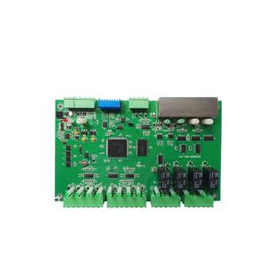
Consignment Prototype PCB Assembly OEM Board
Name: Consignment Prototype PCB Assembly OEM Board
Origin: China
Certified: UL, CE, RoHS
Max Layer:36L
Solder Mask: Green, Black, Blue, Red, Matt Green
Board Thickness: customized
Surface finish: HASL/ lead-free HASL
Lead-Free Prototype PCB Assembly – PCB Manufacturer
Name: Lead-Free Prototype PCB Assembly – PCB Manufacturer
Origin: china
Certified: UL, CE, RoHS
Number of Layers: 6-layer
Base Material: FR-4
Copper Thickness: 0.5-3OZ
Board thickness: customized
- PCB Assembly Capability
- PCB Assembly Equipment
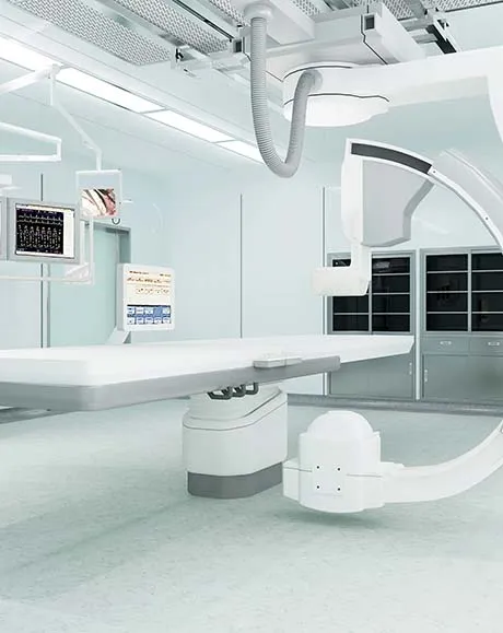
The Prototype PCB Assembly is the perfect solution for turning your circuit designs into functional prototypes swiftly and efficiently. With our state-of-the-art assembly process and expert technicians, we ensure the highest quality and precision in every step. Whether you’re a hobbyist, engineer, or entrepreneur, our PCB assembly service caters to all your prototyping needs.
Our team is well-equipped to handle complex designs and components, including surface mount devices (SMDs), through-hole components, and fine-pitch integrated circuits. We follow stringent quality control measures to guarantee optimal performance and reliability of your prototypes.
Advantages of Prototype PCB Assembly:
- Time-saving: With our Prototype PCB Assembly service, you can significantly reduce the time required to assemble and test your circuit boards. Our efficient processes and experienced team ensure quick turnaround times, allowing you to accelerate your product development cycle.
- Cost-effective: By outsourcing your PCB assembly needs to us, you can save on expensive equipment, specialized personnel, and infrastructure costs. We provide affordable assembly services without compromising on quality.
- Expertise: Our team of skilled technicians has extensive experience in PCB assembly. They possess the knowledge and expertise to handle complex designs, troubleshoot issues, and ensure optimal performance of your prototypes.
- Quality assurance: We adhere to strict quality standards throughout the assembly process. Each prototype undergoes rigorous inspection and testing to ensure it meets your specifications and performs flawlessly.
- Flexibility: We offer flexible assembly options, allowing you to choose the most suitable service for your project requirements. Whether you need a small batch or a larger production run, we can accommodate your needs.
| SMT capacity: 19 million points/day | ||
| Testing Equipment | X-RAY Nondestructive Tester, First Piece Tester, AOI Automatic Optical Tester, ICT Tester, BGA Rework Station | |
| Placement speed | Chip placement speed (at best conditions) 0.036 S/piece | |
| Mounted Component Specifications | Pasteable smallest package | |
| Minimum device accuracy | ||
| IC type chip accuracy | ||
| Mounted PCB Specifications | Substrate size | |
| Substrate thickness | ||
| throw rate | 1. Resistance-capacitance ratio 0.3% | |
| 2. IC type without throwing material | ||
| Board Type | POP/common board/FPC/rigid-flex board/metal substrate | |
| DIP daily production capacity | ||
| DIP plug-in production line | 50000 points/day | |
| DIP post welding production line | 20000 points/day | |
| DIP test production line | 50000pcs PCBA/day | |
| Assembly processing capability | ||
| The company has more than 10 advanced assembly production lines, dust-free and anti-static air-conditioning workshop, TP dust-free workshop, equipped with aging room, test room, functional test isolation room, advanced and perfect equipment, can carry out various product assembly, packaging, testing, Aging, etc. production. Monthly production capacity can reach 150,000 to 300,000 sets/month | ||
| PCBA processing capability | ||
| project | Mass processing capability | Small batch processing capability |
| Number of layers (max) | 2-18 | 20-30 |
| Plate type | FR-4, Ceramic Sheet, Aluminum Base Sheet PTFE, Halogen Free Sheet, High Tg Sheet | PTFE, PPO, PPE |
| Rogers,etc Teflon | E-65, ect | |
| Sheet mixing | 4 layers – 6 layers | 6th floor – 8th floor |
| biggest size | 610mm X 1100mm | / |
| Dimensional Accuracy | ±0.13mm | ±0.10mm |
| Plate thickness range | 0.2mm–6.00mm | 0.2mm–8.00mm |
| Thickness tolerance ( t≥0.8mm) | ±8% | ±5% |
| Thickness tolerance (t<0.8mm) | ±10% | ±8% |
| Media thickness | 0.076mm–6.00mm | 0.076mm–0.100mm |
| Minimum line width | 0.10mm | 0.075mm |
| Minimum spacing | 0.10mm | 0.075mm |
| Outer copper thickness | 8.75um–175um | 8.75um–280um |
| Inner layer copper thickness | 17.5um–175um | 0.15mm–0.25mm |
| Drilling hole diameter (mechanical drill) | 0.25mm–6.00mm | 0.15mm–0.25mm |
| Hole diameter (mechanical drill) | 0.20mm–6.00mm | 0.10mm–0.20mm |
| Hole Tolerance (Mechanical Drill) | 0.05mm | / |
| Hole tolerance (mechanical drill) | 0.075mm | 0.050mm |
| Laser Drilling Aperture | 0.10mm | 0.075mm |
| Plate thickness aperture ratio | 10:1 | 12:1 |
| Solder mask type | Photosensitive green, yellow, black, purple, blue, ink | / |
| Minimum Solder Mask Bridge Width | 0.10mm | 0.075mm |
| Minimum Solder Mask Isolation Ring | 0.05mm | 0.025mm |
| Plug hole diameter | 0.25mm–0.60mm | 0.60mm-0.80mm |
| Impedance tolerance | ±10% | ±5% |
| Surface treatment type | Hot air leveling, chemical nickel gold, immersion silver, electroplated nickel gold, chemical immersion tin, gold finger card board | Immersion Tin, OSP |

Automatic Solder Paste Printing Machine

AOI Optical Inspection

Smt High-Speed Placement Machine

Nitrogen Reflow Soldering

X-Ray

Three Anti-Paint Spraying Machine

SPI Solder Paste Thickness Tester

Automatic Wave Soldering Machine

First Article Inspection
Our complete turnkey PCB assembly service provides a 24 hour quote service for your turnkey PCB assembly order.
Leadsintec cooperates with world-renowned component suppliers to ensure that the source of electronic components is plastic and the authenticity is guaranteed.
It has 7 fully automatic SMT high-speed chip production lines, equipped with ten temperature zone nitrogen reflow ovens, online AOI, SPI, X-RAY and other equipment.
We have complete ISO9001, ISO13485, ISO14001, IATF 16949, UL and other system certifications, and our products meet environmental protection requirements.