

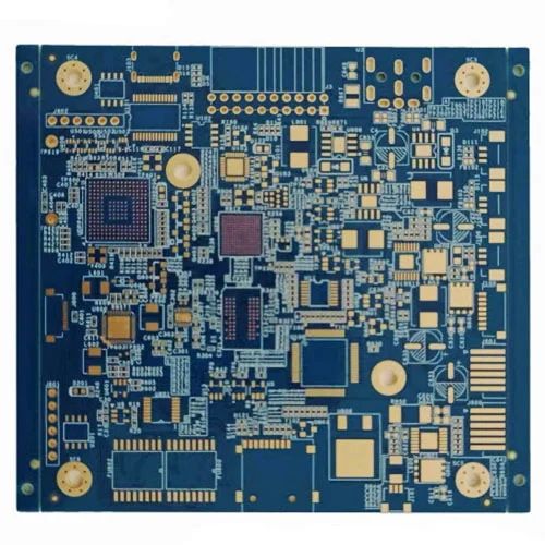
6-layer 1-stage HDI PCB
Name: 6-layer 1-stage HDI PCB
Layers: 1+4+1
Sheet: FR4 Tg150
Plate thickness: 1.6mm
Panel size 105*95mm/1
Outer copper thickness: 35μm
Inner layer copper thickness: 30μm
Minimum through hole: 0.20mm
Minimum blind hole: 0.10mm
Minimum BGA: 0.20mm
Line width line spacing: 3/3mil
Surface Treatment: Immersion Gold 2μ”+OSP
Application field: industrial control
Introducing the exceptional 6-layer 1-stage HDI PCB, a cutting-edge circuit board that revolutionizes electronic design with its advanced features and outstanding performance. This PCB is specifically designed to meet the demands of high-density applications, delivering unrivaled signal integrity, compactness, and reliability.
With its 6-layer construction, this HDI (High-Density Interconnect) PCB offers an ideal solution for complex circuitry. It provides multiple layers for efficient signal routing, minimizing signal interference and ensuring optimal electrical performance. This advanced layer design allows for intricate circuit designs, accommodating a wide range of functionalities and components.
The 1-stage configuration of this HDI PCB ensures streamlined signal flow, maximizing signal integrity and minimizing noise. The single-stage design simplifies the signal path, reducing transmission delays and enhancing overall circuit performance. Whether you’re designing high-speed data communication systems, advanced medical devices, or sophisticated industrial equipment, this PCB offers superior signal transmission capabilities.
Introducing the exceptional 6-layer 1-stage HDI PCB, a cutting-edge circuit board that revolutionizes electronic design with its advanced features and outstanding performance. This PCB is specifically designed to meet the demands of high-density applications, delivering unrivaled signal integrity, compactness, and reliability.
With its 6-layer construction, this HDI (High-Density Interconnect) PCB offers an ideal solution for complex circuitry. It provides multiple layers for efficient signal routing, minimizing signal interference and ensuring optimal electrical performance. This advanced layer design allows for intricate circuit designs, accommodating a wide range of functionalities and components.
The 1-stage configuration of this HDI PCB ensures streamlined signal flow, maximizing signal integrity and minimizing noise. The single-stage design simplifies the signal path, reducing transmission delays and enhancing overall circuit performance.
With the ENIG finish, this rigid flex circuit has the advantages of excellent surface flatness, good oxidation resistance and suitability for movable contacts.
Check our new product 6L 2+N+2 HDI WiFi Module PCB
Name: 6-layer 1-stage HDI PCB
Layers: 1+4+1
Sheet: FR4 Tg150
Plate thickness: 1.6mm
Panel size 105*95mm/1
Outer copper thickness: 35μm
Inner layer copper thickness: 30μm
Minimum through hole: 0.20mm
Minimum blind hole: 0.10mm
Minimum BGA: 0.20mm
Line width line spacing: 3/3mil
Surface Treatment: Immersion Gold 2μ”+OSP
Application field: industrial control
- Previous: 10-layer 3-stage HDI PCB
- Next: 6L 2+N+2 HDI WiFi Module PCB

