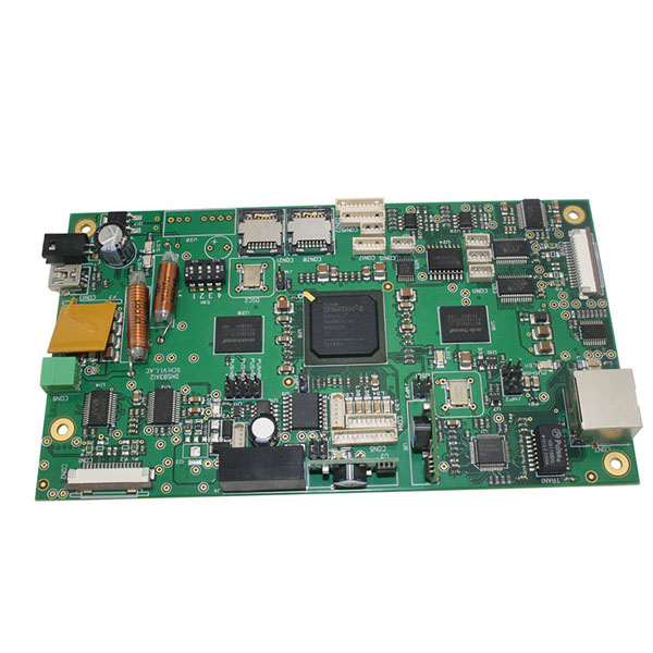
BGA PCB SMT Assembly Electronics PCBA EMS Service
Number of Layer:1,2,4 or 6,upto 18 layer
Order Quantity:1 to 50,000
Board Shape:Retangular,round,slots,cutouts,complex,irregular
Board Type:Rigid, Flexible, Rigid-flexible
Board Material:FR-4 glass epoxy, FR-4 high Tg, Rohs compliant,Aluminum,Rogers,etc.
Board Cutting:Shear,V-score,Tab-routed
Board Thickness:0.2-4.0mm, Flex 0.01-0.25mm
Copper Weight:1.0, 1.5, 2.0 oz
Solder Mask:Double-sided green LPI,Also support Red,White,Yellow,Blue,Black
Silk Screen:Double-sided or single-sided in white,yellow,black,or negative
Silk Screen Min Line Width:0.006” or 0.15mm
Max Board Dimensions:20 inch*20inch or 500mm*500mm
Min Trace/Gap:0.10mm, or 4mils
Min Drill Hole Diameter:0.01”,0.25mm, or 10mils
Surface Finish:HASL,Nickle,Immersion Gold,Immersion Tin,Immersion Silver,OSP,etc.
Board Thickness Tolerance:±10%
Copper Weight Tolerance:± 0.25 oz
Minimal Slot Width:0.12”, 3.0mm, or 120mils
V-Score Depth:20-25% of board thickness
Design File Formate:Gerber RS-274,274D,Eagle and AutoCAD’s DXF,DWG
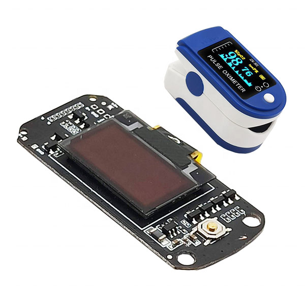
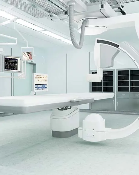
BGA PCB Assembly Factory Manufacture For Pulse Oximeter PCB PCBA one-stop Service
Product Name: PCB Assembly Service
Type: Rigid
Material:FR4, CEM1, CEM3, High Frequency Board,Rogers
Layer:1,2,4,6…20Layer
Shape: Rectangular, Round, Slots, Cutouts, Complex, Irregular
Cutting Shear, V-score, Tab-routed
Board Thickness 0.2-4mm, regular 1.6mm
Copper Thickness:0.5-4oz, regular 1oz
Solder Mask: Green, Red, Blue, Yellow, etc.
Silk Screen: White, Black, etc.
Silk Screen Min Line Width:0.006″ or 0.15mm
Min Trace/Gap:0.1mm or 4mils
Min Drill Hole Diameter 0.01″,0.25mm or 10mils
Surface Finish HASL, ENIG, OSP, etc.
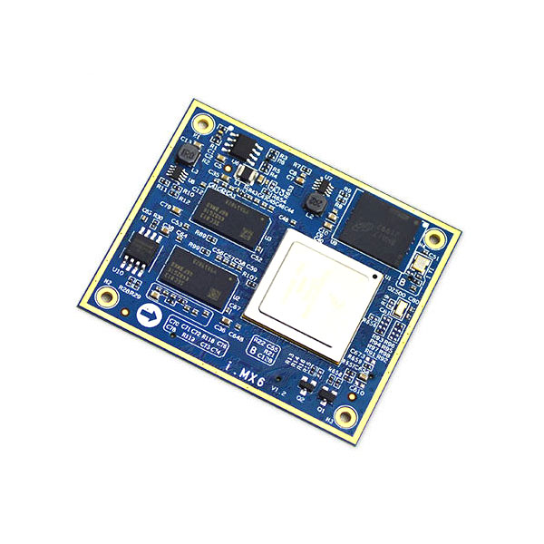
Module ARM Cortex A7 i.MX6 SOM Module BGA Assembly use in IoT Gateway
Name: BGA Assembly
CPU:: ARM Cortex A53 Quad Core 1.28-1.5GHz , MT6739
Operating System: Android 7.0、8.1
Basic Information: GSM 850/900/1800/1900
Screenr: Highest support HD+(1440*720),MIPI interface。
Module Size: 55.5*38.5*3mm
Pin Number: 146pin
Layers: 10 layers ENIG
Flash: 1+8、 2+16、3+32
Wi-Fi: IEEE 802.11 b/g/n, 2.4GHz/5GHz dual-band
GPS: GPS/ GLONASS support AGPS
Bluetooth: BT 4.0、3.0、 2.1 , support BLE
- PCB Assembly Capability
- PCB Assembly Equipment
Introducing BGA (Ball Grid Array) Assembly services, the cutting-edge solution for precise and reliable assembly of complex electronic components. BGA Assembly involves the mounting and soldering of Ball Grid Array packages onto printed circuit boards, providing high-density interconnectivity and enhanced performance for advanced electronic systems.
At our advanced facility, we offer comprehensive BGA Assembly services to meet the demanding requirements of modern electronics. Our state-of-the-art equipment and skilled technicians ensure accurate placement, precise soldering, and meticulous quality control throughout the assembly process.
BGA Assembly is known for its ability to accommodate densely packed components, resulting in compact and efficient circuit designs. By utilizing an array of solder balls instead of traditional leads, BGA packages offer improved electrical performance, reduced signal noise, and enhanced thermal dissipation.
We specialize in handling various BGA types, including micro BGAs, fine-pitch BGAs, and large-scale BGAs, to cater to diverse application needs. Whether it’s consumer electronics, telecommunications, medical devices, or aerospace systems, our BGA services deliver precise and high-performance assemblies.
Advantages of BGA Assembly:
- High-Density Interconnectivity: BGA allows for densely packed components, enabling compact circuit designs and efficient use of PCB space.
- Enhanced Electrical Performance: BGA packages also offer improved electrical performance with reduced signal noise, shorter signal paths, and better impedance control.
- Efficient Thermal Dissipation: The ball grid array configuration facilitates efficient heat dissipation, preventing overheating and also ensuring reliable operation of high-power components.
- Reliable Soldering Connections: BGA employs advanced techniques like reflow soldering and underfill encapsulation to ensure strong and reliable solder joints.
- Meticulous Quality Control: We conduct thorough inspection procedures, including X-ray inspection and also thermal profiling, to verify proper solder joint formation and ensure assembly integrity.
| SMT capacity: 19 million points/day | ||
| Testing Equipment | X-RAY Nondestructive Tester, First Piece Tester, AOI Automatic Optical Tester, ICT Tester, BGA Rework Station | |
| Placement speed | Chip placement speed (at best conditions) 0.036 S/piece | |
| Mounted Component Specifications | Pasteable smallest package | |
| Minimum device accuracy | ||
| IC type chip accuracy | ||
| Mounted PCB Specifications | Substrate size | |
| Substrate thickness | ||
| throw rate | 1. Resistance-capacitance ratio 0.3% | |
| 2. IC type without throwing material | ||
| Board Type | POP/common board/FPC/rigid-flex board/metal substrate | |
| DIP daily production capacity | ||
| DIP plug-in production line | 50000 points/day | |
| DIP post welding production line | 20000 points/day | |
| DIP test production line | 50000pcs PCBA/day | |
| Assembly processing capability | ||
| The company has more than 10 advanced assembly production lines, dust-free and anti-static air-conditioning workshop, TP dust-free workshop, equipped with aging room, test room, functional test isolation room, advanced and perfect equipment, can carry out various product assembly, packaging, testing, Aging, etc. production. Monthly production capacity can reach 150,000 to 300,000 sets/month | ||
| PCBA processing capability | ||
| project | Mass processing capability | Small batch processing capability |
| Number of layers (max) | 2-18 | 20-30 |
| Plate type | FR-4, Ceramic Sheet, Aluminum Base Sheet PTFE, Halogen Free Sheet, High Tg Sheet | PTFE, PPO, PPE |
| Rogers,etc Teflon | E-65, ect | |
| Sheet mixing | 4 layers – 6 layers | 6th floor – 8th floor |
| biggest size | 610mm X 1100mm | / |
| Dimensional Accuracy | ±0.13mm | ±0.10mm |
| Plate thickness range | 0.2mm–6.00mm | 0.2mm–8.00mm |
| Thickness tolerance ( t≥0.8mm) | ±8% | ±5% |
| Thickness tolerance (t<0.8mm) | ±10% | ±8% |
| Media thickness | 0.076mm–6.00mm | 0.076mm–0.100mm |
| Minimum line width | 0.10mm | 0.075mm |
| Minimum spacing | 0.10mm | 0.075mm |
| Outer copper thickness | 8.75um–175um | 8.75um–280um |
| Inner layer copper thickness | 17.5um–175um | 0.15mm–0.25mm |
| Drilling hole diameter (mechanical drill) | 0.25mm–6.00mm | 0.15mm–0.25mm |
| Hole diameter (mechanical drill) | 0.20mm–6.00mm | 0.10mm–0.20mm |
| Hole Tolerance (Mechanical Drill) | 0.05mm | / |
| Hole tolerance (mechanical drill) | 0.075mm | 0.050mm |
| Laser Drilling Aperture | 0.10mm | 0.075mm |
| Plate thickness aperture ratio | 10:1 | 12:1 |
| Solder mask type | Photosensitive green, yellow, black, purple, blue, ink | / |
| Minimum Solder Mask Bridge Width | 0.10mm | 0.075mm |
| Minimum Solder Mask Isolation Ring | 0.05mm | 0.025mm |
| Plug hole diameter | 0.25mm–0.60mm | 0.60mm-0.80mm |
| Impedance tolerance | ±10% | ±5% |
| Surface treatment type | Hot air leveling, chemical nickel gold, immersion silver, electroplated nickel gold, chemical immersion tin, gold finger card board | Immersion Tin, OSP |

Automatic Solder Paste Printing Machine

AOI Optical Inspection

Smt High-Speed Placement Machine

Nitrogen Reflow Soldering

X-Ray

Three Anti-Paint Spraying Machine

SPI Solder Paste Thickness Tester

Automatic Wave Soldering Machine

First Article Inspection
Our complete turnkey PCB assembly service provides a 24 hour quote service for your turnkey PCB assembly order.
Leadsintec cooperates with world-renowned component suppliers to ensure that the source of electronic components is plastic and the authenticity is guaranteed.
It has 7 fully automatic SMT high-speed chip production lines, equipped with ten temperature zone nitrogen reflow ovens, online AOI, SPI, X-RAY and other equipment.
We have complete ISO9001, ISO13485, ISO14001, IATF 16949, UL and other system certifications, and our products meet environmental protection requirements.