

10-layer 3-stage HDI PCB
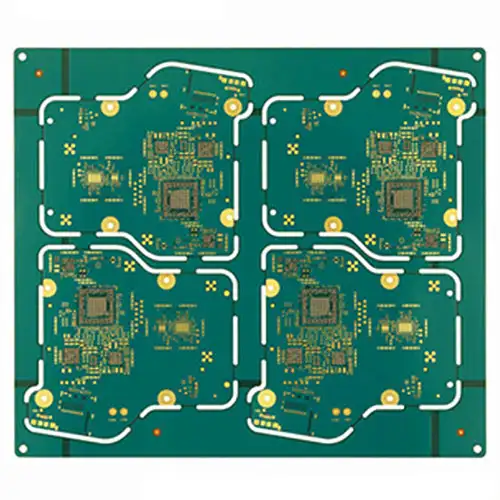
Name: 10-layer 3-stage HDI PCB
Layers: 3+4+3
Sheet: FR4 Tg170
Plate thickness: 1.2mm
Panel size: 126*118mm/4
Outer copper thickness: 35μm
Inner layer copper thickness: 18μm
Minimum through hole: 0.20mm
Minimum blind hole: 0.10mm
Minimum BGA: 0.25mm
Line width and spacing: 2.8/3.2mil
Surface Treatment: Immersion Gold 2μ”+OSP
Introducing the remarkable 10-layer 3-stage HDI PCB, a cutting-edge circuit board that pushes the boundaries of electronic design with its advanced features and exceptional performance. This PCB is specifically engineered to meet the demands of high-density applications, delivering unparalleled signal integrity, compactness, and reliability.
With its 10-layer construction, this 10-layer 3-stage HDI PCB (High-Density Interconnect) PCB offers an ideal solution for complex and highly integrated circuitry. The multiple layers provide ample space for efficient signal routing, minimizing signal interference and ensuring optimal electrical performance. This advanced layer design allows for intricate circuit designs, accommodating a vast array of functionalities and components.
The 3-stage configuration of this HDI PCB takes signal flow to the next level. By dividing the signal path into three stages, it enables enhanced signal transmission and noise reduction. The multi-stage design optimizes the signal path, reducing transmission delays and maximizing overall circuit performance. Whether you’re working on high-speed data communication systems, advanced computing devices, or cutting-edge telecommunications equipment, this PCB empowers you with superior signal transmission capabilities.
The HDI technology employed in this PCB enables a higher component density, enabling more features and functionalities in a smaller form factor. The compact size of the PCB is particularly advantageous in space-constrained applications, where size optimization is crucial. By efficiently utilizing the available space, this PCB allows for sleek and compact electronic device designs without compromising performance.
Name: 10-layer 3-stage HDI PCB
Layers: 3+4+3
Sheet: FR4 Tg170
Plate thickness: 1.2mm
Panel size: 126*118mm/4
Outer copper thickness: 35μm
Inner layer copper thickness: 18μm
Minimum through hole: 0.20mm
Minimum blind hole: 0.10mm
Minimum BGA: 0.25mm
Line width and spacing: 2.8/3.2mil
Surface Treatment: Immersion Gold 2μ”+OSP
- Previous: Cooker hood mother board PCB Prototype
- Next: 6-layer 1-stage HDI PCB

