Single-sided PCBs PCBA assembly board
Name: Single-sided PCBs PCBA assembly board
Origin: China
Certified: UL, CE, RoHS
Copper Thickness: 1/3OZ – 4OZ or Custom
Material: FR4
Solder mask :green, blue, white, red, etc
Board Thickness: customized
Single Double Sided Reflow SMT Soldering
Name: Single Double Sided Reflow SMT Soldering
Origin: China
Certified: UL, CE, RoHS
surface finishing: HASL, HAL-LF, OSP, ENIG
solder mask: green, blue, white, black, grey, red, yellow, purple
material: FR4/Aluminum
Custom ster series ST Lamp PCB single layer
Name: Custom ster series ST Lamp PCB single layer
Origin: China
Certified: UL, CE, RoHS
Surface Finishing: HASL Lead Free
Application: Industrial lamp equipment
material: FR4/Aluminum
copper thickness: 1-5 oz
solder mask: green, blue, white, black, grey, red, yellow, purple
Single-Sided Printed Circuit Board Assembly Oem Pcb & Pcba
Name: Single-Sided Printed Circuit Board Assembly Oem Pcb & Pcba
Origin: China
Certified: UL, CE, RoHS
Surface Finishing: HASL /Lead free
Application: pcba service
Base Material: RF4
Board Thickness: customized
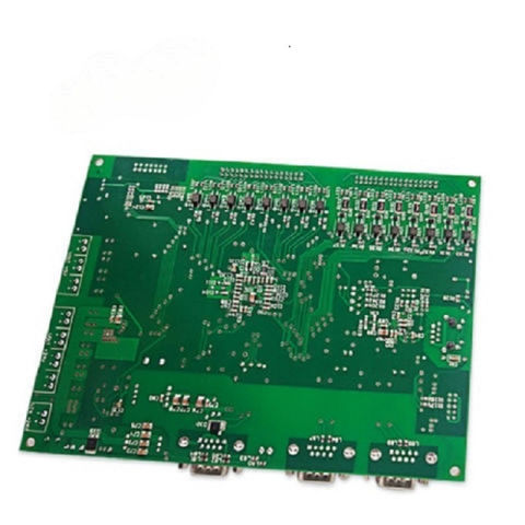
Single layer to multi-layer PCB for Remote Radio Control
Name: Single layer to multi-layer PCB for Remote Radio Control
Origin: China
Certified: UL, CE, RoHS
Surface Finishing: ENIG,HASL,OSP,ENEPIG
Board Size: customized
Solder Mask color: Yellow PI
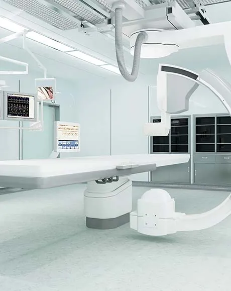
Application: communication

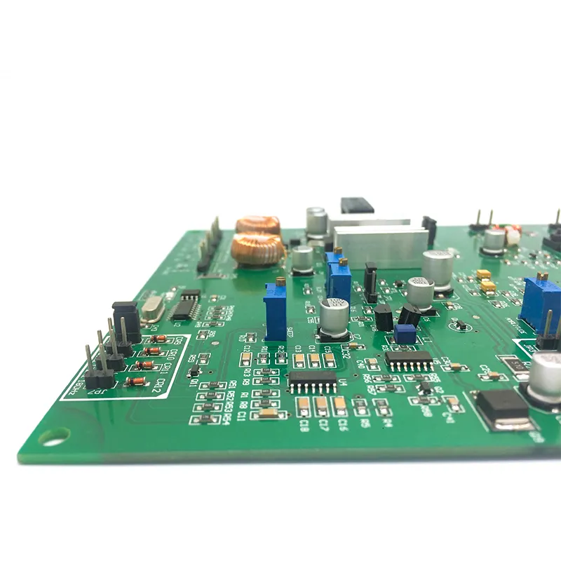
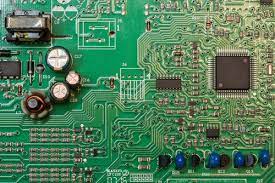
Single-Sided LED Board PCB Assembly-Leadsintec
Name: Single-Sided LED Board PCB Assembly-Leadsintec
Origin: China
Certified: UL, CE, RoHS
Number of Layers: 4-layer
Base Material: FR4, CEM3, PTFE, Aluminum etc
Surface Finishing: HASL, OSP, Immersion Gold/Tin
Solder Mask: Green, Black, Blue, Red, Matt Green
Application: Electronics Device
- PCB Assembly Capability
- PCB Assembly Equipment
Our Single-Sided PCB Assembly service provides a cost-effective and efficient solution for your electronic assembly needs. With our state-of-the-art equipment and skilled technicians, we offer reliable assembly of single-sided printed circuit boards (PCBs) with precision and quality.
Single-sided PCBs are ideal for simple electronic designs and applications that require fewer components. Our assembly process ensures that each component is expertly placed and soldered onto the single copper layer, guaranteeing optimal electrical conductivity and performance.
Advantages of Single-sided PCB assembly:
- Cost-effective: Single-sided PCBs are more economical compared to multi-layered boards. They require fewer materials and involve simpler manufacturing processes, resulting in cost savings without compromising quality.
- Simplified assembly: With only one layer of components and traces, the assembly process is straightforward and streamlined. This reduces the complexity of the assembly, minimizing the chances of errors and facilitating faster production cycles.
- Quick prototyping: Single-sided PCB assembly is an excellent choice for rapid prototyping. With fewer components and simpler designs, you can accelerate the development cycle and quickly validate your electronic concepts.
- Space-efficient: Single-sided PCBs are compact and space-efficient. They are suitable for applications where size constraints are a concern, such as portable devices or space-limited electronic systems.
- Versatility: Despite their simplicity, single-sided PCBs can still accommodate a wide range of electronic components and support various functionalities. They are suitable for applications that do not require complex circuitry or high-density designs.
| SMT capacity: 19 million points/day | ||
| Testing Equipment | X-RAY Nondestructive Tester, First Piece Tester, AOI Automatic Optical Tester, ICT Tester, BGA Rework Station | |
| Placement speed | Chip placement speed (at best conditions) 0.036 S/piece | |
| Mounted Component Specifications | Pasteable smallest package | |
| Minimum device accuracy | ||
| IC type chip accuracy | ||
| Mounted PCB Specifications | Substrate size | |
| Substrate thickness | ||
| throw rate | 1. Resistance-capacitance ratio 0.3% | |
| 2. IC type without throwing material | ||
| Board Type | POP/common board/FPC/rigid-flex board/metal substrate | |
| DIP daily production capacity | ||
| DIP plug-in production line | 50000 points/day | |
| DIP post welding production line | 20000 points/day | |
| DIP test production line | 50000pcs PCBA/day | |
| Assembly processing capability | ||
| The company has more than 10 advanced assembly production lines, dust-free and anti-static air-conditioning workshop, TP dust-free workshop, equipped with aging room, test room, functional test isolation room, advanced and perfect equipment, can carry out various product assembly, packaging, testing, Aging, etc. production. Monthly production capacity can reach 150,000 to 300,000 sets/month | ||
| PCBA processing capability | ||
| project | Mass processing capability | Small batch processing capability |
| Number of layers (max) | 2-18 | 20-30 |
| Plate type | FR-4, Ceramic Sheet, Aluminum Base Sheet PTFE, Halogen Free Sheet, High Tg Sheet | PTFE, PPO, PPE |
| Rogers,etc Teflon | E-65, ect | |
| Sheet mixing | 4 layers – 6 layers | 6th floor – 8th floor |
| biggest size | 610mm X 1100mm | / |
| Dimensional Accuracy | ±0.13mm | ±0.10mm |
| Plate thickness range | 0.2mm–6.00mm | 0.2mm–8.00mm |
| Thickness tolerance ( t≥0.8mm) | ±8% | ±5% |
| Thickness tolerance (t<0.8mm) | ±10% | ±8% |
| Media thickness | 0.076mm–6.00mm | 0.076mm–0.100mm |
| Minimum line width | 0.10mm | 0.075mm |
| Minimum spacing | 0.10mm | 0.075mm |
| Outer copper thickness | 8.75um–175um | 8.75um–280um |
| Inner layer copper thickness | 17.5um–175um | 0.15mm–0.25mm |
| Drilling hole diameter (mechanical drill) | 0.25mm–6.00mm | 0.15mm–0.25mm |
| Hole diameter (mechanical drill) | 0.20mm–6.00mm | 0.10mm–0.20mm |
| Hole Tolerance (Mechanical Drill) | 0.05mm | / |
| Hole tolerance (mechanical drill) | 0.075mm | 0.050mm |
| Laser Drilling Aperture | 0.10mm | 0.075mm |
| Plate thickness aperture ratio | 10:1 | 12:1 |
| Solder mask type | Photosensitive green, yellow, black, purple, blue, ink | / |
| Minimum Solder Mask Bridge Width | 0.10mm | 0.075mm |
| Minimum Solder Mask Isolation Ring | 0.05mm | 0.025mm |
| Plug hole diameter | 0.25mm–0.60mm | 0.60mm-0.80mm |
| Impedance tolerance | ±10% | ±5% |
| Surface treatment type | Hot air leveling, chemical nickel gold, immersion silver, electroplated nickel gold, chemical immersion tin, gold finger card board | Immersion Tin, OSP |

Automatic Solder Paste Printing Machine

AOI Optical Inspection

Smt High-Speed Placement Machine

Nitrogen Reflow Soldering

X-Ray

Three Anti-Paint Spraying Machine

SPI Solder Paste Thickness Tester

Automatic Wave Soldering Machine

First Article Inspection