

Lead-Free Prototype PCB Assembly – PCB Manufacturer
Name: Lead-Free Prototype PCB Assembly – PCB Manufacturer
Origin: china
Certified: UL, CE, RoHS
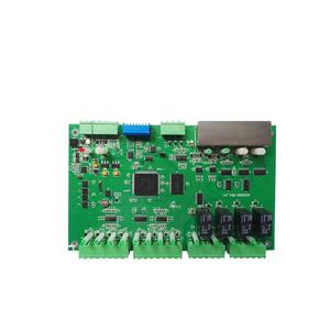
Number of Layers: 6-layer
Base Material: FR-4
Copper Thickness: 0.5-3OZ
Board thickness: customized
Why would a prototype PCB assembly be lead-free?
The lead-free prototype PCB assembly describes the production and assembly of prototype printed circuit boards (PCBs) utilizing lead-free components and materials. Lead-based solder was previously used to connect components to circuit boards in electronic gadgets and PCBs. Prototype without lead Tin-silver-copper or other lead-free solder alloys are some of the alternative solders compounds that are used during PCB manufacturing. Placing electronic components on the PCB, adding solder paste where necessary, and then reflowing the solder to form sturdy electrical connections are all steps in the assembly process.
Prototype PCBs can be created while adhering to environmental requirements by employing lead-free components and lead-free assembly techniques. As a consequence, the electronic gadgets that are produced are safer for both end users and the environment. In order to accomplish appropriate soldering and prevent problems like solder joint dependability, thermal stress, and tin whisker formation, lead-free assembly processes frequently need for certain temperature profiles and considerations.
Maximum Quality and Reliability with Lead-Free Prototype PCB Assembly:
There are various important elements to take into account when it comes to lead-free prototype PCB assembly in order to reach the highest levels of quality and dependability.
Check their suitability:
Ensure that the components you choose are made for lead-free soldering. To guarantee that all components can withstand the higher temperatures needed for lead-free soldering, it is essential to check their suitability.
optimize your PCB design:
To allow lead-free assembly, optimize your PCB design. To improve heat transmission and lower the possibility of solder connection failures, wider traces and bigger pads are used. To avoid solder bridging and shorts, make sure the space between components is enough.
Implement a tightly regulated:
Implement a tightly regulated and meticulously optimized assembling process. Pay close attention to the reflow profile, which includes cooling rates, temperature ramp-up, and peak temperature. To achieve effective melting and reflow, the reflow profile needs to be appropriate for lead-free solder materials.
Superior quality:
Choose a lead-free solder paste of superior quality that is appropriate for your particular application. Make that the solder paste is appropriate for the components being utilized and has adequate wetting and reflow characteristics.
Reliability testing:
Verify that your built PCBs pass the necessary tests by doing reliability testing on them. To evaluate the lead-free assembly’s long-term dependability, this may entail temperature cycling, vibration testing and accelerated ageing tests.
The use of lead-free prototype PCB assembly has various advantages:
- The use of lead in the production of electronics is subject to stringent restrictions in many nations. Adopting lead-free assembly ensures compliance with these laws, enabling you to distribute your products anywhere in the world without running afoul of the law. Lead causes health dangers, particularly during production when employees may come into contact with solder that contains lead. Your staff will operate in a more secure atmosphere with less exposure to dangerous chemicals when lead is removed.
- As people’s knowledge of the environment grows, they are increasingly looking for items that were made with environmentally friendly methods. You meet this need and strengthen your brand’s reputation as an ethical and sustainable business by providing lead-free items.

