

Smt Assembly For Electronic Smart Home
Supplier Type:OEM bluetooth pcba
board thickness:0.2-6mm
Base Material:FR4
Silkscreen Color, Black.white.yellow.red.blue
Number of Layers:1- 40Layers
Testing Service:100% Function Test
Certificate:ISO9001/Iso14001/CE/ROHS
Accuracy of printing:±0.025mm
Components size:0603(Option) L75mm Connector
Pitch:0.15mm
Repeated accuracy:±0.01mm
FOV size:61×45mm
Test speed:9150mm²/Sec
Shootingangle:0-45
Surface Mount Technology (SMT) assembly plays a crucial role in manufacturing electronic smart home devices. SMT allows for the efficient and automated assembly of electronic components onto printed circuit boards (PCBs), which are the building blocks of most electronic devices. Here’s an overview of how SMT assembly is used in the production of electronic smart home devices:
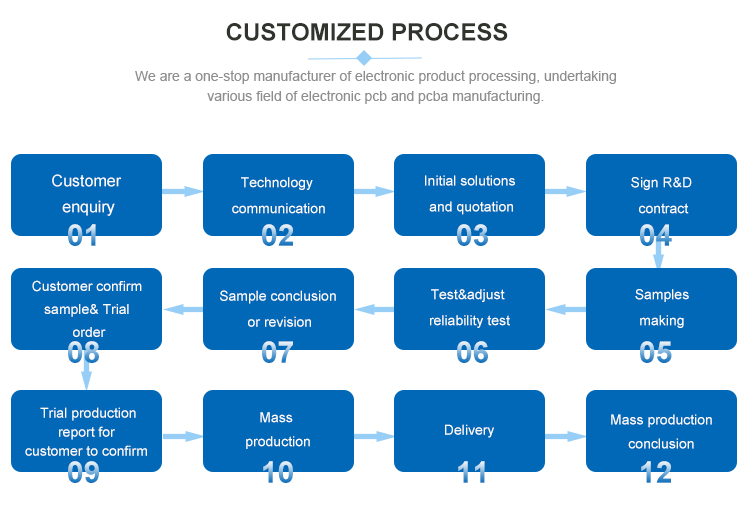
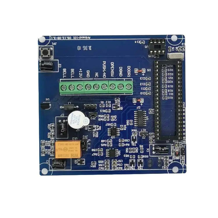
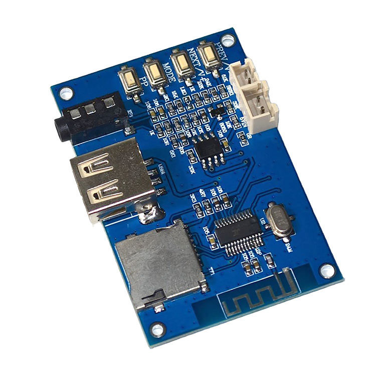
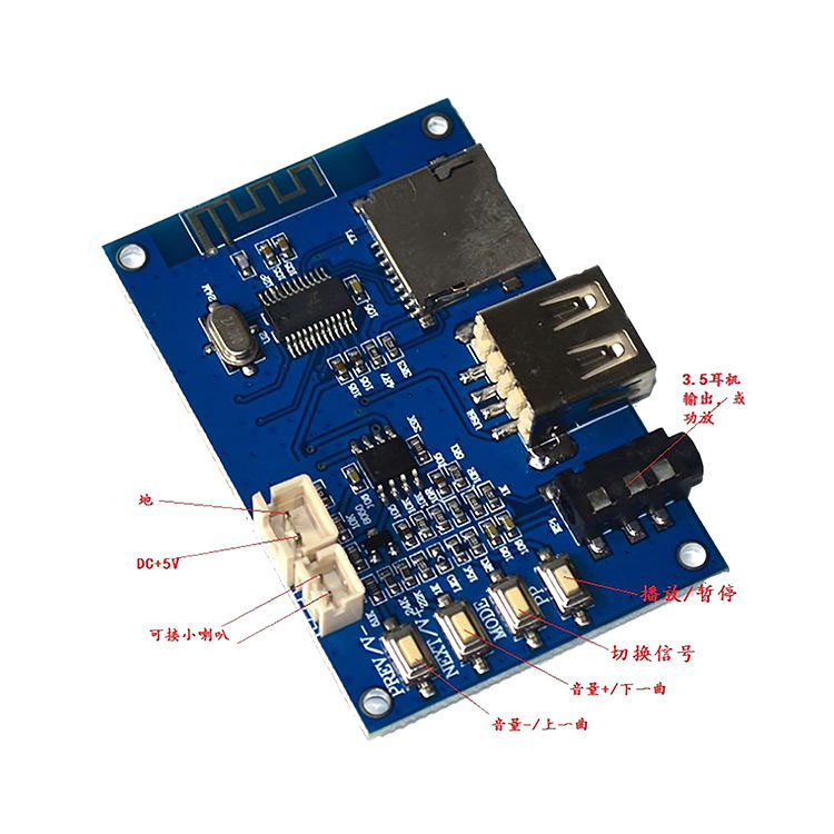
- PCB Design: The first step is to design the PCB layout, which involves placing components and creating the necessary circuit traces. Smart home devices typically consist of various components such as microcontrollers, sensors, wireless modules, connectors, and passive components.
- Component Selection: Once the PCB design is complete, appropriate components are selected based on the device’s functionality and performance requirements. These components need to be compatible with SMT assembly processes, meaning they have surface mount packages, such as small outline integrated circuits (SOIC), quad flat packages (QFP), or ball grid arrays (BGAs).
- SMT Assembly Equipment: SMT assembly requires specialized equipment. The key machines include pick-and-place machines, solder paste printers, and reflow ovens. Pick-and-place machines accurately position the components on the PCB based on the design specifications. Solder paste printers apply solder paste to the PCB pads, and the components are then placed onto the paste. Reflow ovens melt the solder paste, creating a permanent electrical connection between the components and the PCB.
- Quality Control: Throughout the assembly process, quality control measures are implemented to ensure the integrity of the assembled boards. Automated optical inspection (AOI) systems and X-ray inspection are commonly used to detect any assembly defects, such as misaligned components, solder bridging, or insufficient solder joints.
- Testing and Programming: Once the PCBs are assembled, they undergo functional testing to verify their performance. Smart home devices may require additional programming or firmware installation, which is typically done using automated programming systems.
- Final Assembly: After testing and programming, the assembled PCBs are integrated into the final product enclosure, along with any other necessary components like displays, buttons, or external connectors.
- Quality Assurance: The final product undergoes thorough quality assurance testing to ensure it meets the required specifications and functions as intended. This may involve testing various features, connectivity options, and compatibility with smart home ecosystems.
- Packaging and Shipping: Once the smart home devices pass all quality checks, they are packaged and prepared for shipping to distributors or end customers.
Supplier Type:OEM bluetooth pcba
board thickness:0.2-6mm
Base Material:FR4
Silkscreen Color, Black.white.yellow.red.blue
Number of Layers:1- 40Layers
Testing Service:100% Function Test
Certificate:ISO9001/Iso14001/CE/ROHS
Accuracy of printing:±0.025mm
Components size:0603(Option) L75mm Connector
Pitch:0.15mm
Repeated accuracy:±0.01mm
FOV size:61×45mm
Test speed:9150mm²/Sec
Shootingangle:0-45

