

Blue Tooth Pcb Smt Circuit Board Electronic Customized
Supplier Type:OEM bluetooth pcba
board thickness:0.2-6mm
Base Material:FR4
Silkscreen Color, Black.white.yellow.red.blue
Number of Layers:1- 40Layers
Testing Service:100% Function Test
Certificate:ISO9001/Iso14001/CE/ROHS
Accuracy of printing:±0.025mm
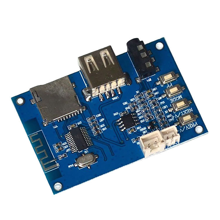
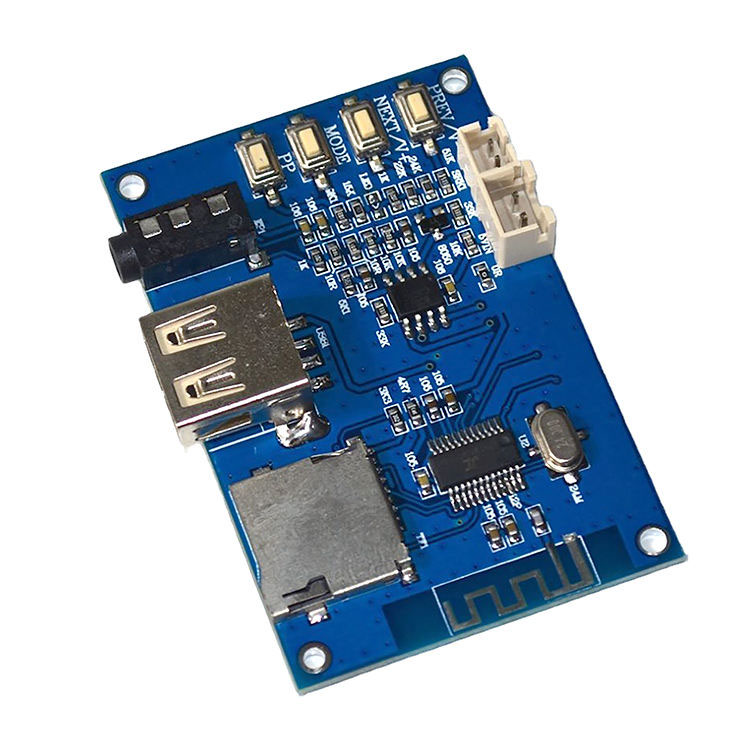
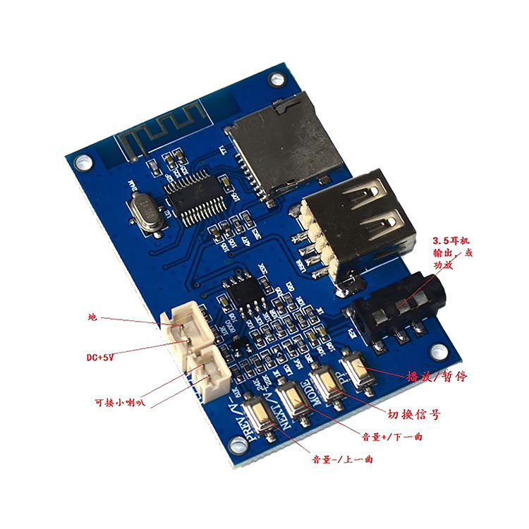
Components size:0603(Option) L75mm Connector
Pitch:0.15mm
Repeated accuracy:±0.01mm
FOV size:61×45mm
Test speed:9150mm²/Sec
Shootingangle:0-45
If you’re looking for a custom Bluetooth PCB (Printed Circuit Board) for surface mount technology (SMT), there are several options available to you. Here’s a general overview of the process and considerations involved in getting a customized Bluetooth PCB:
- Design: Start by defining your specific requirements for the Bluetooth PCB. Consider factors such as the desired Bluetooth version (e.g., Bluetooth 4.0, 5.0), range, power consumption, and any additional features you need.
- Schematic and Layout: Create a schematic diagram that represents the circuit connections and components. Then, design the PCB layout, placing the components and routing the traces based on the schematic. You can use software tools like Altium Designer, Eagle, KiCad, or others for this purpose.
- Manufacturer Selection: Choose a PCB manufacturer that offers customized services and specializes in SMT assembly. Ensure that they have experience working with Bluetooth technology and can meet your specific requirements.
- PCB Manufacturing: Submit your design files to the manufacturer for fabrication. They will produce the PCB according to your specifications, including the number of layers, dimensions, and any additional features like solder mask and silkscreen.
- Component Sourcing: Identify the required components for your Bluetooth PCB. Depending on your preference, you can either provide the components to the manufacturer, or they can source them for you. Ensure that all components are compatible with SMT assembly.
- SMT Assembly: Once the PCBs are fabricated, the manufacturer will proceed with SMT assembly. This process involves mounting the surface-mount components onto the PCB using pick-and-place machines, soldering them using reflow ovens, and inspecting the final product for quality control.
- Testing: After assembly, the PCBs should undergo thorough testing to ensure they meet the required functionality and performance. This can include functional testing, Bluetooth connectivity testing, and other relevant tests.
- Iteration and Production: If necessary, iterate on the design and testing phases until you achieve the desired results. Once the prototype is approved, you can move forward with mass production of the Bluetooth PCBs.
It’s important to note that the process outlined above provides a general overview, and the specifics may vary depending on your requirements and the chosen manufacturer. Working closely with the manufacturer during the design and manufacturing stages will help ensure that your customized Bluetooth PCB meets your expectations.
Supplier Type:OEM bluetooth pcba
board thickness:0.2-6mm
Base Material:FR4
Silkscreen Color, Black.white.yellow.red.blue
Number of Layers:1- 40Layers
Testing Service:100% Function Test
Certificate:ISO9001/Iso14001/CE/ROHS
Accuracy of printing:±0.025mm
Components size:0603(Option) L75mm Connector
Pitch:0.15mm
Repeated accuracy:±0.01mm
FOV size:61×45mm
Test speed:9150mm²/Sec
Shootingangle:0-45

