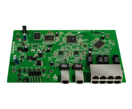
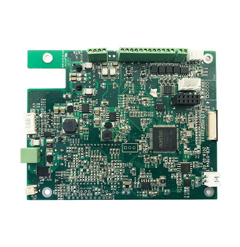
PCB Assembly BGA: The Basics You Need to Know
If you are looking to manufacture a printed circuit board (PCB) with a high-density component, you may want to consider Ball Grid Array (BGA) assembly. BGA assembly is a method of attaching integrated circuits to a PCB using a grid of small balls of solder instead of traditional pins. This method allows for more connections to be made in a smaller space, making it ideal for complex PCB designs.

BGA assembly can be a cost-effective solution for your PCB manufacturing needs. The assembly process is automated, which can reduce labor costs and increase efficiency. Additionally, BGA packages are smaller than traditional pin packages, which can reduce the size of your PCB and overall manufacturing costs. BGA assembly can also increase the reliability of your PCB by reducing the risk of solder joint failure.
Overview of BGA Technology

If you are involved in the assembly of printed circuit boards (PCBs), it is likely that you have come across the term Ball Grid Array (BGA). BGA is a packaging technology that has been widely adopted in the electronics industry due to its numerous advantages over traditional packaging methods.
BGA Packaging Types
BGA packages come in different types, including Flip Chip BGA (FCBGA), Ball Grid Array (BGA), and Land Grid Array (LGA). FCBGA is soldered directly to the circuit board using a special process, eliminating the need for pins or leads. BGA is one of the most commonly used types of BGA PCB assembly and consists of a grid of solder balls arranged in an array. LGA is similar to BGA, but instead of having a grid of solder balls, it has an array of lands.
Advantages of BGA over Traditional Packaging
One of the main advantages of BGA over traditional packaging methods is its higher pin density. BGA packages feature a multitude of spherical bumps on their surface, providing a vast number of connections to the board. This allows for more connections in a smaller space, making it possible to pack more functionality into a smaller area.
Another advantage of BGA is its better thermal performance. The solder balls used in BGA packages provide a larger surface area for heat dissipation, making it possible to dissipate heat more efficiently. This is particularly important in high-performance applications where heat dissipation is critical.
BGA packages are also more reliable than traditional packaging methods. The solder balls used in BGA packages provide a more robust connection to the board, making them less prone to mechanical failure. This is particularly important in applications where the PCB will be subjected to vibration or other mechanical stresses.
In summary, BGA technology is an advanced packaging technique that has been widely adopted in the electronics industry due to its numerous advantages over traditional packaging methods. BGA packages come in different types, including FCBGA, BGA, and LGA. The advantages of BGA over traditional packaging methods include higher pin density, better thermal performance, and greater reliability.
PCB Assembly Process for BGA

When it comes to assembling a PCB with a BGA component, there are three main steps to follow: Solder Paste Application, Component Placement, and Reflow Soldering.
Solder Paste Application
The first step in assembling a PCB with a BGA component is to apply solder paste to the pads on the PCB. This is typically done using a stencil that is placed over the PCB and aligned with the pads. The solder paste is then applied to the stencil and spread over the pads using a squeegee.
Component Placement
Once the solder paste has been applied to the pads, the BGA component can be placed onto the PCB. This is typically done using automated pick-and-place machines, which are programmed to place the component onto the correct pads with a high degree of accuracy.
Reflow Soldering
The final step in assembling a PCB with a BGA component is to reflow solder the component onto the PCB. This is done by heating the PCB and the BGA component in a reflow oven, which causes the solder paste to melt and flow, creating a strong and reliable connection between the BGA component and the PCB.
During the reflow process, it’s important to ensure that the temperature and time profiles are carefully controlled to prevent damage to the BGA component or the PCB. This is typically done using specialized software that monitors the temperature and time profiles during the reflow process.
Overall, the PCB assembly process for BGA components is a complex and precise process that requires careful attention to detail and a high degree of accuracy. However, by following the three main steps of solder paste application, component placement, and reflow soldering, you can ensure that your PCB with a BGA component is assembled correctly and reliably.
Inspection and Quality Control
When it comes to PCB assembly BGA, inspection and quality control are crucial steps to ensure the reliability and functionality of the final product. There are different methods and techniques available to inspect and control the quality of BGA solder joints, including X-Ray Inspection and Automated Optical Inspection (AOI).
X-Ray Inspection
X-Ray Inspection is a non-destructive method used to inspect the quality of BGA solder joints. This technique allows the inspection of the internal structure of the solder joints, which is not visible to the naked eye. X-Ray Inspection can detect various defects such as voids, cracks, and insufficient solder, which can affect the reliability and functionality of the PCB.
X-Ray Inspection is an effective method for inspecting BGA solder joints because it can detect defects that are not visible to the naked eye. This technique is commonly used in the electronics manufacturing industry to ensure the quality and reliability of BGA solder joints.
Automated Optical Inspection (AOI)
Automated Optical Inspection (AOI) is another method used to inspect the quality of BGA solder joints. AOI uses cameras and software to inspect the PCB for defects such as missing components, polarity, and solder defects. This technique is faster than X-Ray Inspection and can detect defects that are visible to the naked eye.
AOI is an efficient method for inspecting BGA solder joints because it can quickly detect defects and can be easily integrated into the PCB assembly process. This technique is commonly used in electronics manufacturing to ensure the quality and reliability of BGA solder joints.
Inspection and quality control are crucial steps in PCB assembly BGA to ensure the reliability and functionality of the final product. X-Ray Inspection and Automated Optical Inspection (AOI) are two effective methods used to inspect the quality of BGA solder joints. By using these methods, you can ensure that your PCB assembly BGA is of high quality and meets the required standards.
Rework and Repair of BGA
BGA or Ball Grid Array is a type of surface mount packaging for integrated circuits that is commonly used in PCB assembly. BGA packages have become increasingly popular due to their high pin count and small size. However, BGA rework and repair can be a challenging process, and it requires specialized equipment and skills to perform properly.
BGA Rework Stations
BGA rework stations are specialized equipment used to remove and replace BGA components on PCBs. These stations typically consist of a heating element, a vacuum system, and a controller. The heating element is used to heat the PCB and the BGA component to a temperature that melts the solder, allowing the component to be removed. The vacuum system is used to remove the component once the solder has melted. The controller is used to control the temperature and other parameters during the rework process.
When selecting a BGA rework station, it is important to consider the size of the components that will be reworked, as well as the number of components that will be reworked at once. The station should also be capable of heating the PCB and component to the required temperature without damaging the PCB or other components on the board.
BGA Reballing Process
BGA reballing is the process of replacing the solder balls on a BGA component. This process is typically performed after the component has been removed from the PCB. The reballing process involves applying new solder balls to the component using solder paste. The component is then reflowed to melt the solder and attach the balls to the component.
The reballing process can be performed manually or using specialized equipment. Manual reballing involves applying the solder balls to the component by hand, while automated reballing uses equipment to apply the balls more precisely. Automated reballing is typically faster and more accurate than manual reballing, but it requires specialized equipment.
BGA rework and repair is a challenging process that requires specialized equipment and skills. When selecting a BGA rework station, it is important to consider the size and number of components that will be reworked. The BGA reballing process can be performed manually or using specialized equipment, and both methods have their advantages and disadvantages.
Design Considerations for BGA Assembly
When designing a PCB for BGA assembly, there are several key considerations to keep in mind. These include PCB pad design and thermal management.
PCB Pad Design
PCB pad design is crucial for successful BGA assembly. The pad size and pitch of the BGA package should match the corresponding pads on the PCB. The pad size should be slightly larger than the solder ball diameter to allow for proper solder wetting and adhesion. The pitch, or distance between the centers of adjacent pads, should be chosen based on the specific BGA package being used.
It is also important to consider the number of layers in the PCB stackup. The BGA pinout and I/O count can be used to determine the number of layers needed in a PCB stackup. Once you have determined the trace width needed to route controlled impedance lines into the BGA, you can determine the layer thickness needed to maintain impedance.
Thermal Management
Thermal management is another important consideration for BGA assembly. BGAs generate more heat than other types of packages due to their high pin density. Therefore, it is important to ensure that the PCB design includes adequate thermal management.
One common approach is to use thermal vias, which are plated-through holes that extend from the top to the bottom of the PCB. These vias allow heat to be dissipated from the BGA package to the bottom of the PCB, where a heatsink or other cooling mechanism can be attached.
Another approach is to use a metal core PCB, which has a layer of metal (usually aluminum or copper) sandwiched between layers of insulating material. The metal core provides a highly conductive path for heat to flow away from the BGA package.
Overall, careful consideration of PCB pad design and thermal management is crucial for successful BGA assembly. By following these guidelines, you can ensure that your BGA assembly is reliable and performs optimally.


