

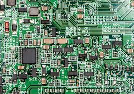
Scanning Device Medical PCB – One Stop Service in China
Name: Scanning Device Medical PCB – One Stop Service in China
Origin: China
Certified: UL, CE, RoSH
Copper Thickness: 1 oz
Surface Finishing: ENIG, HASL, OSP, etc.
Solder Mask: Blue
Layers: 4 Layers
Why is Medical PCB Scanning Device One Stop Service in China?
One-stop services in China can meet clients’ unique requirements, including small-scale production, prototyping, and customization. Greater flexibility and quick turnaround times are made possible by the capacity to manage several facets of the production process for Scanning Device Medical PCB under one roof. There are several reasons why scanning equipment, notably medical PCBs, is provided in China as a one-stop solution.
-
Scanning Device Medical PCB has good manufacturing capability:
China has sophisticated manufacturing skills, which include the capacity to produce PCBs and electronic components. The nation is renowned for its robust infrastructure, knowledgeable workforce, and efficient industrial techniques. Due to these elements, it is the perfect place to offer comprehensive services for scanning medical PCBs.
-
Integration of the supply chain:
The electronics manufacturing supply chain ecosystem in China is well-established and interconnected. Suppliers of raw materials, component producers, PCB assembly facilities, and testing and inspection services are all part of this ecosystem. The availability of one-stop services is made possible by the effective coordination and expedited procedures made possible by the proximity of all these components.
-
Cost-Effectiveness:
China’s manufacturing sector is noted for its affordable prices compared to other locations. Chinese businesses may streamline their operations, save administrative expenses, and pass the cost savings down to clients by offering one-stop services.
-
Technical know-how:
China has invested much in research and development, creating a highly qualified workforce with experience in PCB fabrication and electronics. The accessibility of skilled engineers, technicians, and experts helps produce scanning devices and the PCBs that go with them in an effective and high-quality manner.
-
Conformity with Regulations:
China has created regulatory frameworks and standards for the production of medical devices, assuring conformity with global standards for quality and safety. Chinese businesses may successfully negotiate these rules by providing one-stop services and giving clients dependable and legal items.
How are Scanning Device Medical PCBs Innovating the Medical Industry?
-
Miniaturization and Portability:
Smaller and more portable scanning equipment has been made possible by medical PCBs. Thanks to improved PCB designs and manufacturing methods, complex functionality may now be integrated into small devices. As a result, portable ultrasound equipment, handheld diagnostic instruments, and other scanning tools have been made easier to use in various healthcare settings, including rural or resource-constrained places.
Scanning Device Medical PCB are essential parts of scanning machines that enhance the effectiveness and precision of medical diagnostics. These PCBs are made to analyze high-speed data quickly, amplify signals, reduce noise, and precisely regulate scanning processes. Medical PCBs enhance patient outcomes by enhancing signal processing and data collecting capabilities. This allows for quicker and more accurate diagnosis.
-
Scanning Device Medical PCB offers Cost-Effectiveness:
Scanner equipment costs have decreased due to innovations in medical PCB manufacturing. Production of medical PCBs is now more productive and inexpensive because of improved manufacturing procedures, materials, and assembly methods. This affordability makes scanning equipment more broadly available, allowing medical institutions and experts to embrace these technologies more.

