

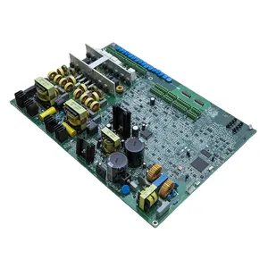
Phone System Double-sided PCB-Leadsintec
Name: Phone System Double-sided PCB-Leadsintec
Base Material: FR4
Copper Thickness: 1oz
Surface Finishing: HASL,ENIG,OSP
Number of Layers: 2
Application: Electronics Device
Solder mask color: Blue. green. red. black .white .etc
Various processes of Phone System Double-sided PCB Assembly:
The process of creating and putting together double-sided printed circuit boards (PCBs) for phone systems is referred to as phone system double-sided PCB. A phone system normally consists of numerous electrical parts and circuits installed on PCBs to enable communication and other functions. Circuitry and component placement are on both sides of a double-sided printed circuit board (PCB), enabling more sophisticated circuitry and a greater component density. There are various phases in the assembling process:
-
PCB Design:
Using specialized software, the PCB is designed while considering the needs and demands of the phone system. Component, trace, and route location are all part of the design.
-
PCB Fabrication:
After the PCB design has been completed, fabrication work starts. It entails etching a copper-clad laminate material to produce the desired circuit layout. After that, holes are drilled into the board to make room for component placement.
-
Component placement:
Component insertion on double-sided PCBs uses surface mount technology (SMT). Automated pick-and-place machines precisely position and solder the components onto the board using solder paste or adhesive.
-
Soldering:
To firmly fasten the components to the PCB, soldering includes heating the solder paste or adhesive. Reflow soldering, in which the PCB is passed through a hot oven, or wave soldering, in which the PCB is passed over a wave of molten solder, are two methods that may be used to accomplish this.
-
Inspection and testing:
The PCB is thoroughly inspected after assembly to guarantee correct component placement, high-quality soldering, and electrical continuity. Functional testing and automated optical inspection (AOI) methods are frequently used to find any flaws or defects.
-
Finalization:
The PCB assembly is finished by adding a conformal coating or other protective measures to increase its longevity and resilience to environmental conditions after passing inspection and testing.
The Advantages of Double-Sided PCB Assembly for Phone Systems:
-
Compact Design:
Double-sided PCBs enable larger component densities and more intricate circuitry. Phone system designers may use the available space best by using both sides of the board, leading to a more compact and effective design. This is especially crucial given the limited capacity of mobile phones and other portable devices.
-
Superior Signal Integrity:
When compared to single-sided PCBs, double-sided PCBs offer superior signal integrity. Designers may optimize signal routing and shorten signal lines by placing components and traces on both sides of the board, which lowers the likelihood of interference, crosstalk, and signal degradation. The phone system performs better and is more dependable as a result.
Double-sided PCBs’ more area and complexity make it possible to incorporate phone systems with more sophisticated features and functions. It allows incorporation of extra parts like sensors, connections, audio circuits, power management circuits, and others. Because of this, phone systems may now provide various features, including camera modules, biometric sensors, wireless networking, and different multimedia applications.
-
Cost-effective Production:
Phone System Double-sided PCB is now a common and reliable production method. It thereby gains from economies of scale and effective production methods. Automated pick-and-place devices and other cutting-edge manufacturing techniques are now readily available, streamlining the assembly process and lowering labor costs while boosting total production efficiency. This enables phone system makers to use double-sided PCB assembly as a cost-effective option.
-
Easier Troubleshooting and Repair:
Compared to multi-layer PCBs, double-sided PCBs are simpler to troubleshoot and repair. Technicians can quickly access and see possible problems, such as broken components or solder joints because components and traces are visible on both sides of the board. This makes repairs easier, shortens downtime, and improves the phone system’s general maintenance and serviceability.

