

Lightwave Communications PCB Board
Name: Lightwave Communications PCB Board
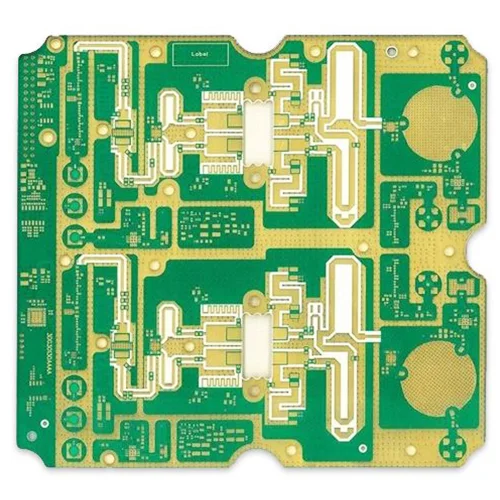
Layers: 6L
material: TU872+R4350B
Board Thicknes: 1.8 mm
Copper Thicknes: 35/35/35/35um
Smallest Hole Diameter: 0.20mm
Surface Treatment: ENIG(2U”)
Technical Feature: Vacuum Plugging, Blind buried via
Applications
Ground receiving equipment
Introducing the Lightwave Communications PCB Board, a high-performance solution designed specifically for the demanding requirements of lightwave communication systems. This advanced PCB board is optimized to deliver exceptional signal integrity, and reliable performance in optical communication applications.
The Lightwave Communications PCB Board is engineered with specialized materials and design considerations to support the transmission of light signals with minimal attenuation and distortion. It provides excellent dielectric properties and low insertion loss. This enables efficient and accurate signal propagation over long distances.
This PCB board is designed to accommodate a wide range of lightwave communication technologies. This includes fiber optic networks, optical transceivers, optical amplifiers, and other optical communication devices. It offers precise control over impedance matching. It also allows for seamless integration with lightwave components and minimizing signal reflections.
With its high-speed signal transmission capabilities, the Lightwave Communications PCB Board is suitable for applications requiring high data rates, such as high-definition video streaming, data centers, and telecommunications networks. It also ensures reliable data transfer and low bit error rates. This contributes to the overall performance and efficiency of your lightwave communication system.
High-Speed Circuits for Lightwave Communication provides the latest information on circuit design, measurement results, applications, and product development. It also covers electronic and optoelectronic circuits for transmission, reception and crosspoint switching. These circuits are implemented using a variety of state-of-the-art IC technologies, including Si BJT, GaAs MESFET, HEMT, HBT, and InP HEMT and HBT.
Name: Lightwave Communications PCB Board
Layers: 6L
material: TU872+R4350B
Board Thicknes: 1.8 mm
Copper Thicknes: 35/35/35/35um
Smallest Hole Diameter: 0.20mm
Surface Treatment: ENIG(2U”)
Technical Feature: Vacuum Plugging, Blind buried via
Applications
Ground receiving equipment
- Previous: High Frequency Hybrid PCB Board
- Next: Rogers RO4350B High Frequency Board

