

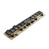
HDI Low Volume PCB Assembly especially for Equipment
Name: HDI Low Volume PCB Assembly especially for Equipment
Origin: China
Certified: UL, CE, RoHS
Copper Thickness: 4 oz
Application field: LED LIPS
Copper Thickness: 4 oz
Board thickness: Mass production: 394mil(10mm) Samples: 17.5mm
Layer: 1-64 L
Surface finish: HASL, OSP, Immersion Gold/Silver/Tin, ENIG, Gold Finger
What is HDI Low Volume PCB Assembly?
A specialized electronic manufacturing service called Low Volume PCB Assembly is designed to produce printed circuit boards (PCBs) in small batches. It is meant to be used for prototypes, small-batch production runs, or PCBs that are produced specifically for a customer. HDI Low Volume PCB Assembly provides flexible, customizable, and rapid turnaround times for applications requiring smaller manufacturing volumes. Applications including research and development, proof-of-concept prototypes, specialized machinery, and niche markets are perfect fits for it.
The process of constructing printed circuit boards (PCBs) with high-density interconnect technology in small quantities is known as HDI (High-Density Interconnect) Low Volume PCB Assembly. By packing more parts and connections into a smaller space, HDI technology enables the miniaturization and expansion of functionality of electronic products. Low volume PCB assembly is the process of creating PCBs in small batches, usually starting with a few prototypes and ending with a single production run. High-volume PCB assembly, on the other hand, entails a sizable size of PCB fabrication for mass-market goods.
Important Characteristics and Implications of Low-Volume PCB Assembly:
-
Customization and Flexibility:
Low Volume Assembly provides flexibility in allowing for specialized designs, particular needs, and design revisions. It enables the introduction of distinctive elements, specialized features, and personalized layouts to suit the project’s particular requirements.
-
Cost-Effectiveness:
Because it avoids the high upfront expenses connected with large-scale production techniques, low volume assembly is cost-effective for modest production volumes. It permits cost reduction without compromising quality. Because of this, it may be used for initiatives with little funding or market demand.
-
Quick Turnaround:
Compared to high-volume production, low-volume assembly often offers quicker turnaround times. The assembly may be finished more quickly with simpler procedures and smaller manufacturing lines. This makes it possible to quickly deliver prototypes or small-batch PCB orders.
-
Design Validation and Prototyping:
Low Volume Assembly is a great option for design verification and prototype development. Before going to full-scale manufacturing, it enables engineers and designers to test and make adjustments to their concepts. Additionally, it offers a chance to spot and take care of any design flaws, operational difficulties, or performance enhancements early on.
-
Quality Control and testing of low volume PCB assembly:
HDI Low Volume PCB Assembly still follows stringent quality control and testing procedures, despite the reduced manufacturing volumes. Additionally, this guarantees that each constructed PCB satisfies the functional and specification requirements. Functional testing, automated optical inspection (AOI), visual inspection, and other pertinent quality assurance procedures are all examples of testing. Leadsintec is a UL and ISO9001 certified business. With our EMS assembly capabilities, we can create 120,000,000 components per month and 20,000 square meters of PCBs per month.
Uses for HDI Low Volume PCB Assembly:
- A printed circuit board with high-density interconnections is assembled in low manufacturing numbers and is referred to as an HDI (High-Density Interconnect) Low Volume PCB. When complicated circuitry is needed yet there is not much room available, this technology is frequently employed in a variety of applications. HDI low volume PCB assembly is frequently utilized in products like wearable tech, tablets, smartphones, and smart watches.
- HDI technology may be used to create these devices’ compact form factors and high functionality requirements. Strict size and performance constraints sometimes apply to medical equipment. Medical device miniaturization with the required functionality is made possible by HDI low volume PCB assembly. Implants used in medicine, diagnostic tools, and portable monitoring equipment are a few examples.

