

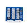
High Speed Design Through Hole PCB Assembly
Name: High Speed Design Through Hole PCB Assembly
Origin: China
Certified: UL, CE, RoHS
Copper Thickness: 1OZ,2OZ,3OZ 4OZ 5OZ Customization
Board thickness: 0.3-3.5mm
Surface Finishing: OSP, HASL, Immersion gold, Immersion Tin etc.
Solder mask: Green, Black, Blue, Red, white etc.
The brief introductions of High Speed Design through Hole PCB Assembly:
The technique of putting together printed circuit boards (PCBs) that are particularly made to handle high-speed signals and data transfer is known as high-speed design through hole PCB assembly. Through-hole technology, which includes inserting component leads through the board’s drilled holes, is used to put and solder electronic components on a PCB. PCBs are built with careful consideration of signal integrity, impedance matching, and minimizing electromagnetic interference (EMI) in high-speed design applications.
For high-frequency signals to be transmitted effectively and reliably, several design factors must be taken into account. In high-speed design, through-hole technology is used to provide reliable electrical connections and better signal integrity. Typically, through-hole components are utilized for parts that need to handle more power, be more durable, or be more reliable. Electronic components with wire leads are put during assembly into pre-drilled holes in the PCB.
In order to make strong electrical connections, the leads are then soldered on the opposite side. For some components, through-hole assembly offers a more secure and durable mechanical connection than surface mount technology (SMT). Specialized tools, such wave soldering machines or selective soldering systems, are needed for high-speed design through-hole PCB assembly in order to accomplish accurate component positioning and exact soldering. By adhering to industry standards and best practices, careful consideration is given to minimizing signal loss, managing impedance, and lowering EMI.
What do High Speed Design through hole PCB Assemblies serve?
There are several uses for High Speed Design through hole PCB assembly in the development and production of electrical circuits.
Signal Integrity:
To maintain accurate and dependable data transmission, high-speed designs must carefully take signal integrity into account. Techniques for through-hole PCB assembly are used to reduce signal deterioration, including electromagnetic interference (EMI), crosstalk, and signal reflections. Signal integrity is maintained via appropriate component placement, controlled impedance routing, and grounding strategies.
High-Frequency Performance:
Because through-hole components have shorter lead lengths and less parasitic effects than surface-mount components, they can provide greater high-frequency performance. To get the best electrical performance, certain components, including connections, high-frequency filters, and high-power components, are frequently installed via holes in high-speed designs.
Power Distribution:
High-speed circuits frequently require a lot of power, and through-hole components can make power distribution more effective. To manage high current flow and give reliable power to crucial components, components like big capacitors, inductors, and power connections are frequently installed through holes.
What applications High Speed Design through hole PCB Assembly is used for in RF and microwave technologies?
- Assembling printed circuit boards (PCBs) that are intended to handle high-frequency signals and data transfer is referred to as high-speed design through-hole PCB assembly. Despite the fact that through-hole technology is typically linked with older electronic components, it may still be utilized in high-speed designs for certain applications. Signal integrity and impedance control are crucial in RF and microwave technology, and through-hole components can be helpful in these applications.
- Due to their widespread availability in through-hole packages, several RF components, such as connectors, filters, and amplifiers, are appropriate for high-speed PCB designs. For high-power applications where components must manage large currents and effectively dissipate heat, through-hole PCB construction is frequently recommended. Power electronics, motor control systems, and industrial automation equipment are some of these applications.

