PCB Assembly Process Steps: A Comprehensive Guide
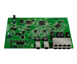
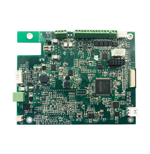
If you’re interested in electronics manufacturing, you’ve likely heard of the PCB assembly process. This process involves assembling and soldering components onto a printed circuit board (PCB) to create a functional electronic device. The PCB assembly process is a critical step in the production of electronic devices, and it requires precision and attention to detail to ensure the final product meets the necessary standards.

There are several steps involved in the PCB assembly process, each of which is crucial to the final product’s success. These steps include designing the PCB, ordering components, preparing the PCB, placing the components, soldering the components, and testing the final product. Each step requires specific tools, techniques, and expertise to ensure the final product is of high quality and meets the required specifications. In the following sections, we’ll explore each of these steps in more detail and explain why they’re essential to the PCB assembly process.
Design and Layout

The design and layout phase is an essential step in the PCB assembly process. It involves creating a schematic capture and PCB layout that will serve as a blueprint for the manufacturing process.
Schematic Capture
In the schematic capture phase, you will use software such as Altium, Protel, Orcad, KiCad, or other similar tools to create a circuit pattern. This pattern will define the electrical connections between components and the overall functionality of the circuit.
It is important to ensure that the schematic capture is accurate and complete. Any errors or omissions at this stage can result in costly delays and rework later in the process. It is also crucial to consider the manufacturability of the design at this stage.
PCB Layout
In the PCB layout phase, you will use the schematic capture to create the physical layout of the circuit board. This involves placing components and routing traces to create the desired electrical connections.
When creating the PCB layout, it is essential to consider factors such as signal integrity, power distribution, and thermal management. You will also need to ensure that the layout complies with design for manufacturability (DFM) guidelines to avoid issues during the manufacturing process.
Overall, the design and layout phase is critical to the success of the PCB assembly process. By creating an accurate and manufacturable design, you can ensure that the manufacturing process runs smoothly and that the final product meets your requirements.
Materials and Components Preparation

Before starting the PCB assembly process, you need to prepare all the materials and components required. This involves selecting the right materials and sourcing the components from reliable suppliers. In this section, we will discuss the two important steps involved in materials and components preparation: material selection and component sourcing.
Material Selection
The first step in materials preparation is selecting the right materials for your PCB. The materials you choose will depend on the requirements of your project, such as the operating temperature, frequency, and environment. Some of the commonly used materials for PCBs include FR-4, CEM-1, CEM-3, and Rogers.
It is important to choose high-quality materials that are suitable for your project. Using low-quality materials can result in poor performance, reduced lifespan, and even safety hazards. Therefore, it is recommended to choose materials that meet industry standards and have been tested for quality and reliability.
Component Sourcing
The second step in materials preparation is component sourcing. This involves sourcing all the components required for your PCB assembly process from reliable suppliers. The components you need will depend on the requirements of your project, such as the type of ICs, resistors, capacitors, and connectors.
It is important to source components from reliable suppliers who provide high-quality components. Using low-quality components can result in poor performance, reduced lifespan, and even safety hazards. Therefore, it is recommended to source components from suppliers who have a good reputation in the industry and provide components that meet industry standards.
In summary, materials and components preparation is an important step in the PCB assembly process. It involves selecting the right materials and sourcing high-quality components from reliable suppliers. By taking these steps, you can ensure that your PCB assembly process is successful and your project meets your requirements.
PCB Fabrication
Once the PCB design is finalized, the next step in the PCB assembly process is the fabrication of the actual board. This process typically involves several steps, including etching, drilling, and plating.
Etching
Etching is the process of removing unwanted copper from the surface of the board using a chemical solution. This process is used to create the copper traces that will eventually become the electrical connections between components on the board. The etching process typically involves applying a layer of resist material to the board, exposing the areas where copper is desired, and then applying the etching solution to remove the unwanted copper.
Drilling
Once the copper traces have been etched onto the board, the next step is to drill holes for the components and vias. The drilling process typically involves using a computer-controlled drill to create precise holes in the board. The size and location of the holes are determined by the PCB design and are critical to ensuring proper placement and alignment of the components.
Plating
The final step in the PCB fabrication process is plating. This process involves depositing a thin layer of metal onto the surface of the board to improve its conductivity and protect it from oxidation. The plating process typically involves applying a layer of copper to the board using an electroplating process. Once the copper layer has been applied, a layer of tin or other metal is typically applied to protect the copper from oxidation.
Overall, the PCB fabrication process is a critical step in the PCB assembly process. Each step must be carefully executed to ensure that the final board is of high quality and meets the specifications of the PCB design. By following the proper fabrication process, you can ensure that your PCBs are reliable and perform as intended.
Assembly and Soldering
Once the PCB design is complete and the components are ready, it’s time to assemble and solder the components onto the board. This step is crucial to ensure that the PCB functions as intended. In this section, we will discuss the different assembly and soldering techniques used in the PCB assembly process.
Surface Mount Technology
Surface mount technology (SMT) is a popular method used to mount electronic components onto a PCB. In this method, the components are placed directly onto the surface of the board. SMT is a faster and more efficient method compared to through-hole technology. SMT components are smaller, and the placement process is automated, which results in a higher placement accuracy.
Through-Hole Technology
Through-hole technology (THT) is another method used to mount electronic components onto a PCB. In this method, the components are inserted through holes drilled into the board. THT components are larger and require more manual labor to place them onto the board. THT is a slower and more time-consuming method compared to SMT.
Reflow Soldering
Reflow soldering is the process of melting and re-solidifying solder paste to join the components to the board. In this process, the board is heated to a specific temperature, and the solder paste melts, creating a bond between the component and the board. Reflow soldering is a popular method used in SMT assembly as it allows for precise control over the soldering process.
In conclusion, the assembly and soldering process is a critical step in the PCB assembly process. The different techniques used in this process, such as SMT, THT, and reflow soldering, have their advantages and disadvantages. It’s essential to choose the right method based on the PCB design and the components used.
Testing and Quality Control
After the PCB assembly process is complete, it is important to ensure that the PCB is functioning correctly and meets the necessary quality standards. This is done through testing and quality control measures.
Automated Optical Inspection
One method of testing is Automated Optical Inspection (AOI), which involves using a machine to scan the PCB for defects. AOI machines use high-resolution cameras to capture images of the PCB and then analyze them for any defects or issues. This method is fast and accurate, making it a popular choice for PCB testing.
During AOI, the machine checks for various issues such as missing components, misplaced components, soldering defects, and incorrect polarity. If any issues are detected, the machine will flag them for further inspection and correction.
Functional Testing
Another important method of testing is functional testing, which involves testing the PCB’s functionality under real-world conditions. This is done by applying power to the PCB and testing its various functions to ensure they are working correctly.
Functional testing can be done manually or through the use of specialized equipment. This method of testing is important because it ensures that the PCB is working correctly and will perform as intended in its intended application.
In addition to testing, quality control measures are also important to ensure the PCB meets the necessary quality standards. This includes ensuring that the components used in the PCB are of high quality, that the PCB meets all necessary regulatory requirements, and that the PCB is properly labeled and documented.
By implementing these testing and quality control measures, you can ensure that your PCB assembly process is producing high-quality PCBs that will meet the necessary standards for their intended applications.
Packaging and Shipping
Once the PCB assembly process is complete, the next step is packaging and shipping the PCBs to the customer. This step is crucial to ensure that the PCBs reach their destination safely. Proper packaging is required to prevent damage during shipping. The packaging must also meet the requirements of the transportation method being used. For example, packaging that can withstand high vibration and shock is usually required.
There are different types of packaging materials available for PCBs. Some of the commonly used materials include antistatic bags, foam inserts, and corrugated boxes. Antistatic bags are used to prevent electrostatic discharge (ESD) that can damage the PCB. Foam inserts are used to provide cushioning and protect the PCB from impact during shipping. Corrugated boxes are used as outer packaging to provide additional protection to the PCB.
Before packaging the PCB, it is important to inspect it thoroughly. The PCB should be checked for any defects or damages that may have occurred during the assembly process. Any defects or damages should be repaired before packaging the PCB.
Once the PCB has been inspected and repaired (if necessary), it can be packaged. The PCB should be placed in an antistatic bag and then placed in a foam insert. The foam insert should be placed in a corrugated box and sealed with tape. The box should be labeled with the customer’s address and any other relevant information.
Finally, the PCB should be shipped using a reliable transportation method. The transportation method should be chosen based on the destination, weight, and size of the PCB. It is important to choose a transportation method that can deliver the PCB safely and on time.
In summary, packaging and shipping is the final step in the PCB assembly process. Proper packaging is required to prevent damage during shipping. The PCB should be inspected and repaired (if necessary) before packaging. The PCB should be packaged using antistatic bags, foam inserts, and corrugated boxes. The transportation method should be chosen based on the destination, weight, and size of the PCB.


