


BGA PCB Assembly: Everything You Need to Know
If you’re looking to learn about BGA PCB assembly, you’ve come to the right place. BGA, or Ball Grid Array, is a type of surface mount package used for integrated circuits. BGA packages feature a grid of solder balls on their underside, which are used to form electrical connections with the PCB.
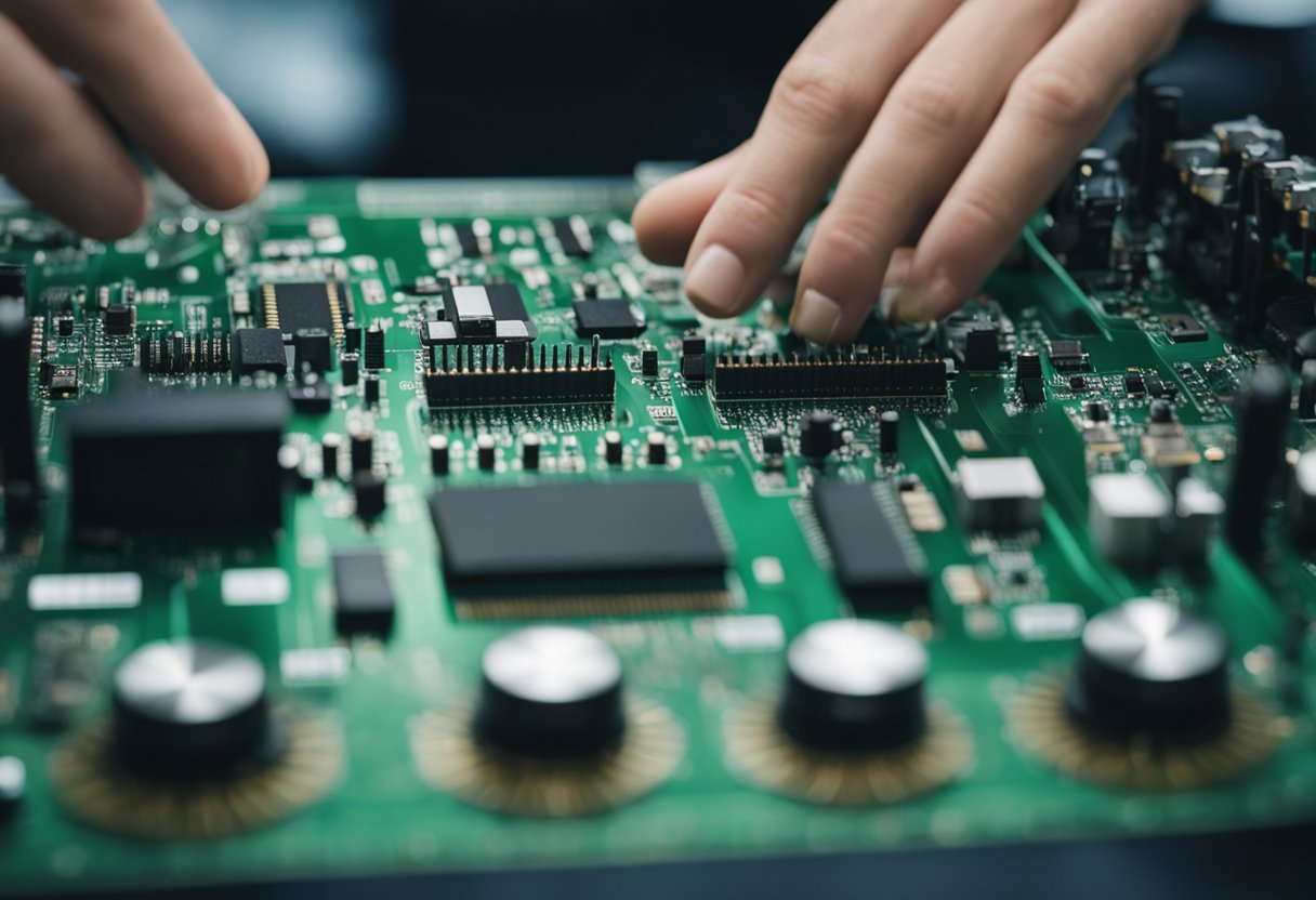
BGA PCB assembly is a process that involves soldering a BGA package onto a printed circuit board. The process is complex and requires specialized equipment and expertise. BGA assembly is used in a wide range of applications, from consumer electronics to aerospace and defense.
In this article, we’ll cover the basics of BGA PCB assembly, including the advantages and disadvantages of using BGA packages, the different types of BGA packages available, and the process of BGA assembly. Whether you’re a student, hobbyist, or professional engineer, this article will provide you with a solid foundation for understanding BGA PCB assembly.
BGA PCB Assembly Overview
If you’re looking to assemble a printed circuit board (PCB), you may come across the term BGA, which stands for Ball Grid Array. BGA is a type of surface mount technology (SMT) used in electronic manufacturing. In this section, we will provide an overview of BGA PCB assembly, including the components and materials used, as well as the types of BGA packages available.
Components and Materials
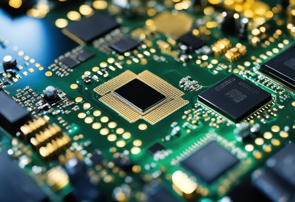
BGA PCB assembly involves the use of several components and materials. The components include the BGA package, which is a surface-mounted integrated circuit (IC) that uses small solder balls at its bottom instead of conventional pins. Other components include resistors, capacitors, and other ICs. The materials used in BGA PCB assembly include the PCB itself, solder paste, and flux.
Types of BGA Packages
There are several types of BGA packages available, including ceramic BGAs, plastic BGAs, and tape BGAs. Ceramic BGAs are made of a ceramic material and are known for their durability and reliability. Plastic BGAs are made of a plastic material and are less expensive than ceramic BGAs. Tape BGAs are a type of plastic BGA that uses a tape substrate instead of a traditional PCB.
In addition to these types of BGA packages, there are also different types of BGA assemblies, including:
- Area array BGA
- Column grid array BGA
- Fine pitch BGA
- Micro BGA
Each of these BGA assemblies has its own unique characteristics and specifications.
Overall, BGA PCB assembly is a popular choice for electronic manufacturing due to its compact size, high density, and low assembly costs. By understanding the components and materials used in BGA PCB assembly, as well as the types of BGA packages available, you can make an informed decision when it comes to assembling your own PCB.
Design Considerations
When designing a BGA PCB assembly, there are several important considerations to keep in mind to ensure successful implementation. These include BGA footprint design, thermal management, and signal integrity.
BGA Footprint Design
The BGA footprint design is a crucial aspect of BGA PCB assembly. The size and shape of the pads, vias, and solder mask openings must be carefully designed to ensure proper soldering and electrical connections. The PCB designer must consider the pitch, ball diameter, and pin count of the BGA device when designing the footprint. It is important to use the manufacturer’s recommended footprint as a starting point and modify it as necessary.
Thermal Management
Thermal management is another important consideration in BGA PCB assembly. The high-density nature of BGA packages can lead to higher power densities, which can cause overheating and damage to the device. Proper thermal management techniques such as adding thermal vias, using thermal pads, and increasing copper pour areas can help to dissipate heat and prevent damage to the device.
Signal Integrity
Signal integrity is critical in BGA PCB assembly, as high-speed signals can be affected by the parasitic capacitance and inductance of the BGA package. The PCB designer must carefully route high-speed signals to minimize signal loss and interference. The use of controlled impedance routing and proper termination techniques can also help to maintain signal integrity.
In summary, when designing a BGA PCB assembly, it is important to consider the BGA footprint design, thermal management, and signal integrity. By following these design considerations, you can ensure a successful BGA PCB assembly that meets your performance and reliability requirements.
Assembly Process
BGA (Ball Grid Array) assembly is a complex process that involves several steps to ensure a successful outcome. In this section, we will discuss the four main stages of the assembly process: Solder Paste Application, Component Placement, Reflow Soldering, and Inspection and Quality Control.
Solder Paste Application
The first step in BGA assembly is to apply solder paste to the PCB. This is typically done using a stencil that is aligned with the PCB pads. The solder paste is then applied to the stencil and pushed through the openings onto the pads. The stencil is then removed, leaving a thin layer of solder paste on the pads. It is important to ensure that the correct amount of solder paste is applied, as too much or too little can cause problems during the assembly process.
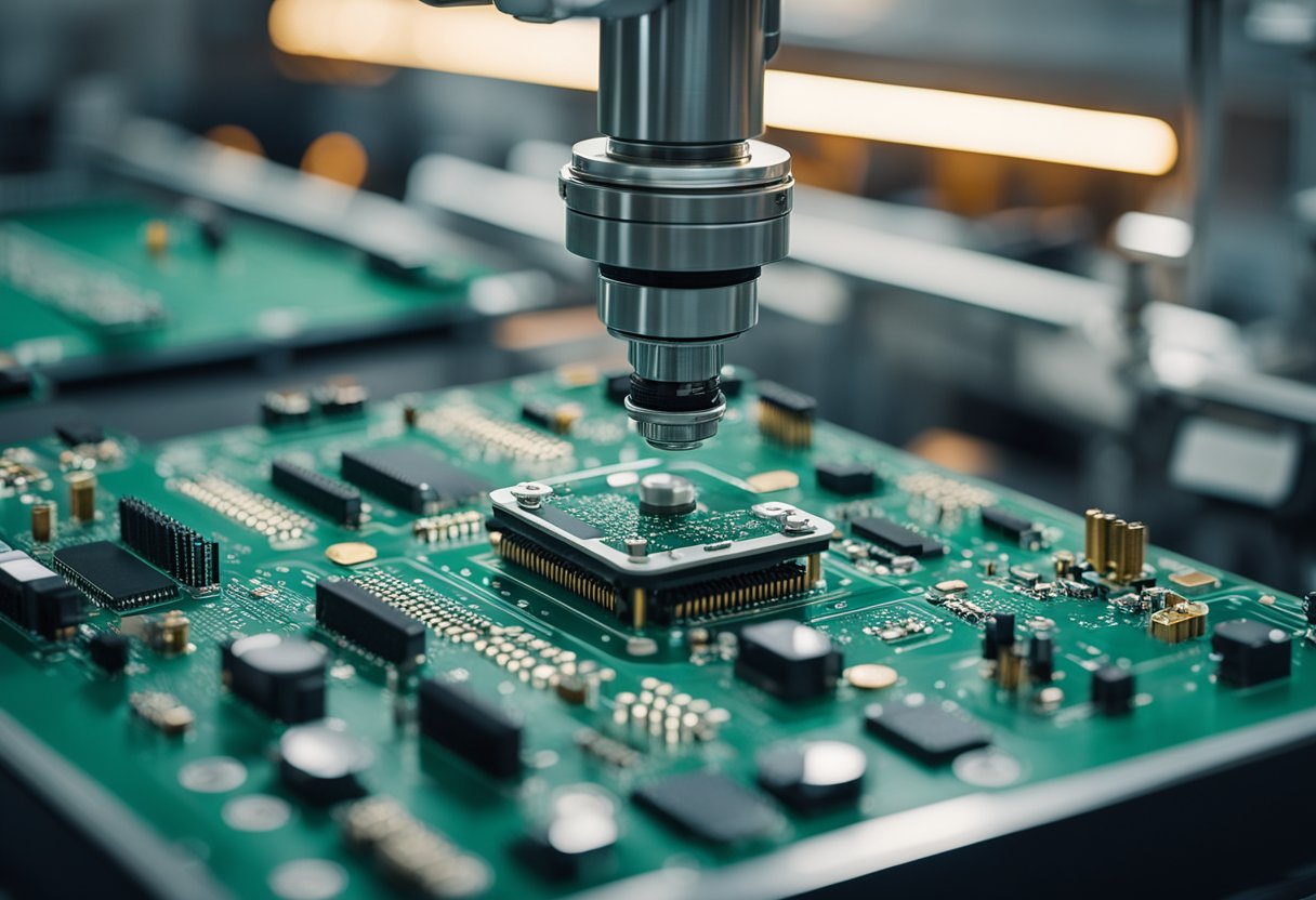
Component Placement
Once the solder paste has been applied, the components are placed onto the PCB. This is typically done using automated pick-and-place machines that are programmed with the correct component positions. The machine picks up each component and places it onto the corresponding pad. It is important to ensure that each component is placed in the correct position and orientation, as mistakes can cause problems during the assembly process.
Reflow Soldering
After the components have been placed, the PCB is heated in a reflow oven to melt the solder paste and create a permanent bond between the components and the PCB. The temperature and time of the reflow process are critical, as they can affect the quality of the solder joints. It is important to ensure that the reflow process is carefully controlled and monitored to ensure a successful outcome.
Inspection and Quality Control
Once the reflow process is complete, the PCB is inspected to ensure that all of the components are properly attached and that there are no defects or soldering issues. This is typically done using automated optical inspection (AOI) machines that can detect defects that are not visible to the naked eye. It is important to ensure that the inspection process is thorough and that any issues are addressed before the PCB is shipped to the customer.
Common Challenges and Solutions
BGA Voiding
One of the most common challenges when it comes to BGA PCB assembly is voiding. Voiding is the formation of gas pockets within the solder joint that can cause defects in the assembly. This can happen due to a variety of reasons such as poor solder paste quality, incorrect reflow profile, or incorrect pad design.
To avoid BGA voiding, it’s essential to use high-quality solder paste with low voiding characteristics. Additionally, the reflow profile should be optimized to ensure that the solder paste melts and solidifies correctly. The pad design should also be optimized to reduce the formation of gas pockets within the solder joint.
Solder Bridging
Another common challenge in BGA PCB assembly is solder bridging. Solder bridging occurs when solder connects two adjacent pads, causing a short circuit. This can happen due to excessive solder paste, incorrect reflow profile, or incorrect pad design.
To avoid solder bridging, it’s essential to use the correct amount of solder paste. The reflow profile should also be optimized to ensure that the solder paste melts and solidifies correctly. The pad design should also be optimized to reduce the possibility of solder bridging.
Pad Cratering
Pad cratering is another common challenge in BGA PCB assembly. Pad cratering is the formation of cracks in the PCB pad that can cause defects in the assembly. This can happen due to a variety of reasons such as poor PCB material quality, incorrect pad design, or excessive thermal stress.
To avoid pad cratering, it’s essential to use high-quality PCB material with good mechanical properties. The pad design should also be optimized to reduce the possibility of pad cratering. Additionally, excessive thermal stress should be avoided by optimizing the reflow profile.
By understanding these common challenges and their solutions, you can ensure a successful BGA PCB assembly process.
Testing and Reliability
When it comes to BGA PCB assembly, testing and reliability are crucial factors to consider. Here are some of the most common testing methods that can ensure your BGA PCB assembly is reliable:
X-Ray Inspection
X-ray inspection is a non-destructive testing method that uses electromagnetic radiation to create images of the internal structure of a BGA PCB assembly. This method is used to check for any defects or faults in the assembly, such as soldering defects, voids, and cracks. X-ray inspection is a quick and efficient way to identify potential issues before the assembly is put into use.
Functional Testing
Functional testing is a type of testing that checks the functionality of the BGA PCB assembly. This type of testing is done to ensure that the assembly works as intended and meets all the necessary requirements. Functional testing can be done manually or through automated testing, depending on the complexity of the assembly.
Environmental Stress Tests
Environmental stress tests are designed to test the BGA PCB assembly’s ability to withstand harsh environmental conditions. These tests simulate extreme temperatures, humidity, and other environmental factors that the assembly may encounter during its lifetime. The purpose of environmental stress tests is to ensure that the assembly can operate reliably in any environment.
Overall, testing and reliability are essential factors to consider when it comes to BGA PCB assembly. By using these testing methods, you can ensure that your assembly is reliable and meets all necessary requirements.
Frequently Asked Questions
How does BGA technology improve PCB performance?
BGA technology improves PCB performance by enabling higher pin density and a smaller form factor. The compact size of BGA components allows for more components to be placed on a single PCB, which can lead to faster processing speeds and increased functionality. Additionally, the ball grid array design of BGA components provides a more robust connection to the PCB, which can improve signal integrity and reduce the risk of failure due to mechanical stress.
What are the challenges of soldering BGA components on a PCB?
Soldering BGA components on a PCB can be challenging due to the small size of the solder balls and the high pin density of the component. In addition, BGA components are often placed on the underside of the PCB, which can make it difficult to inspect the solder joints. To ensure a successful BGA soldering process, it is important to use appropriate equipment and techniques, including precise temperature control, accurate placement, and proper inspection methods.
Can you explain the various BGA package types and their applications?
There are several types of BGA packages, including ceramic, plastic, and tape ball grid array. Ceramic BGA packages are often used in high-performance applications, while plastic BGA packages are more commonly used in consumer electronics. Tape ball grid array packages are typically used in mobile devices due to their small size and low profile. The specific type of BGA package used depends on the requirements of the application.
What are the best practices for BGA PCB design and layout?
To ensure successful BGA PCB design and layout, it is important to consider the size and pitch of the BGA package, the pad size and pitch of the PCB, and the placement of other components on the board. The pad size of the PCB should be slightly larger than the solder ball diameter to allow for proper solder joint formation. Additionally, it is important to minimize the distance between the BGA component and the via to reduce the risk of signal noise.
How is BGA assembly different from traditional SMT processes?
BGA assembly differs from traditional SMT processes in that the solder joints are formed between the BGA component and the PCB, rather than on the surface of the PCB. This requires more precise temperature control and inspection methods to ensure proper solder joint formation. Additionally, BGA components are often placed on the underside of the PCB, which can make inspection more challenging.
What inspection techniques are used to ensure the quality of BGA assembly?
Several inspection techniques are used to ensure the quality of BGA assembly, including X-ray inspection, visual inspection, and automated optical inspection. X-ray inspection is often used to inspect the solder joints of BGA components, as it can provide a clear view of the joints without damaging the component or PCB. Visual inspection and automated optical inspection are also commonly used to detect defects in the solder joints or component placement.

